SWRU596 December   2022


  1. 1Abstract
    1.     Trademarks
  2. 2Getting Started
    1. 2.1 Key Features
    2. 2.2 Kit Contents
    3. 2.3 mmWave Out of Box Demo
  3. 3Hardware
    1. 3.1 Block Diagram
  4. 4EVM Mux Block Diagram
  5. 5PCB Storage and Handling Recommendations:
    1. 5.1 PCB Storage and Handling Recommendations:
    2. 5.2 Higher Power Demanding Applications:
  6. 6XWRL6432BOOST Antenna
    1. 6.1  PCB material
      1. 6.1.1 Transmitter and receiver virtual array
    2. 6.2  Switch Settings
    3. 6.3  LEDs
    4. 6.4  Connectors
    5. 6.5  USB Connector
    6. 6.6  DCA1000 HD Connector
    7. 6.7  Booster Pack Connector for the LaunchPad Connectivity
    8. 6.8  CANFD Connector
    9. 6.9  LIN PHY connection
    10. 6.10 I2C Connections
      1. 6.10.1 EEPROM
    11. 6.11 XDS110 Interface
    12. 6.12 Flashing the Board
    13. 6.13 DCA1000EVM Mode
      1. 6.13.1 RDIF interface for Raw ADC capture
  7. 7Software, Development Tools, and Example Code
    1. 7.1 XWRL6432 Demo Visualization Getting Started
  8. 8TI E2E Community
  9. 9References
    1.     Revision History

EVM Mux Block Diagram

Figure 4-1 shows different muxing options for the digital signals. The device is pin limited to support different features simultaneously; hence various internal IPs and signals are pin multiplexed. EVM provides de-muxing options using various analog mux and sliding switch options. Figure 4-1 shows different muxing switch positions to enable different muxing options to connect to different peripherals.
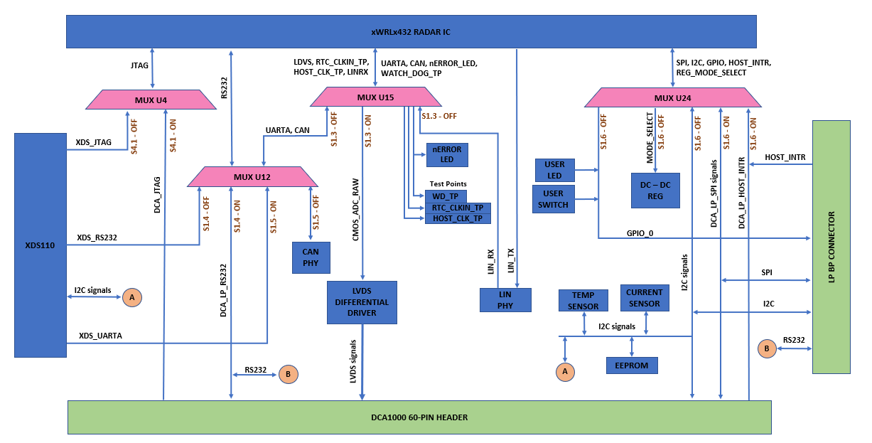
GUID-810025A5-90A0-469A-B3A5-DCB688395C81-low.png Figure 4-1 Muxing options for the EVM