TIDT193 August 2020 – MONTH
3.3 Output Voltage Ripple
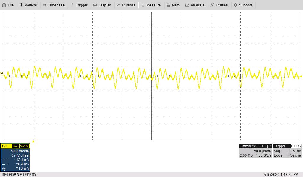
The following image illustrates the output ripple voltage (AC coupled). The input voltage is 18 V and the 14-V output is loaded to 130 mA.
 Figure 3-16 Output Voltage Ripple (AC Coupled) (VOUT: 50 mV/div, 50 μs/div)
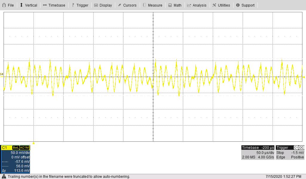
The following image illustrates the output ripple voltage (AC coupled). The input voltage is 30 V and the 14-V output is loaded to 130 mA.
 Figure 3-17 Output Voltage Ripple (AC Coupled) (VOUT: 50 mV/div, 50 μs/div)
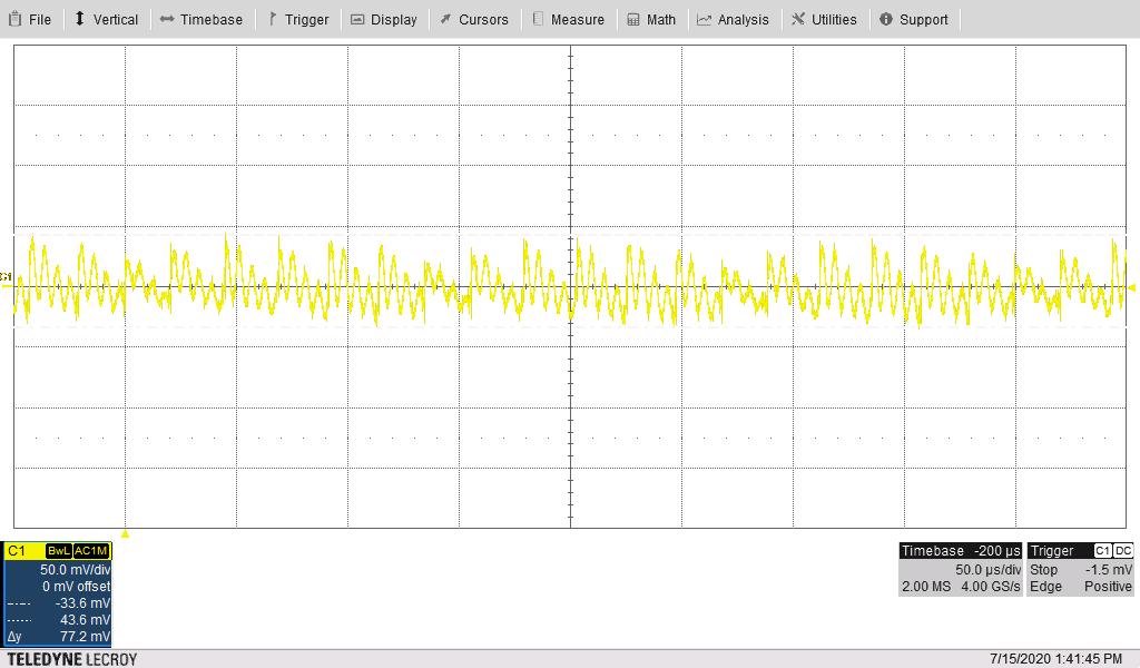
The following image illustrates the output ripple voltage (AC coupled). The input voltage is 120 V and the 14-V output is loaded to 130 mA.
 Figure 3-18 Output Voltage Ripple (AC Coupled) (VOUT: 50 mV/div, 50 μs/div).