TIDT195 September 2020 – MONTH
2.1 Thermal Images
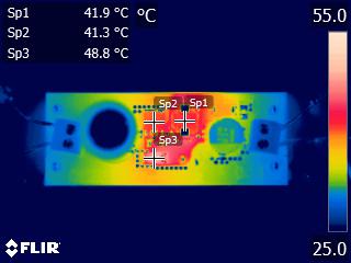
This thermal image shows the operating temperature of the top side of the board with 120 VDC input and 12 V at 400-mA output at room temperature and no air flow.
 Figure 2-1 Top-Side Thermal Image, 120-VDC Input, 12 V at 400-mA Output
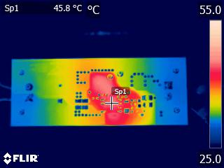
This thermal image shows the operating temperature of the bottom side of the board with 120-VDC input and 12 V at 400-mA output at room temperature and no air flow.
 Figure 2-2 Bottom-Side Thermal Image, 120-VDC Input, 12 V at 400-mA Output.