TIDT195 September   2020  – MONTH 


  1.   Description
  2. 1Test Prerequisites
    1. 1.1 Voltage and Current Requirements
    2. 1.2 Required Equipment
  3. 2Testing and Results
    1. 2.1 Thermal Images
    2. 2.2 Efficiency and Power Dissipation Graphs
    3. 2.3 Efficiency and Power Dissipation Data
    4. 2.4 Voltage Regulation
  4. 3Waveforms
    1. 3.1 Start-up
    2. 3.2 Switch Node
    3. 3.3 Output Voltage Ripple
    4. 3.4 Load Transients
    5. 3.5 Short-Circuit Recovery Response

Short-Circuit Recovery Response

The following image shows the output voltage (RED) recover from a short to ground and the output load current (GREEN). VIN = 100 V and VOUT is 12 V at 400 mA.
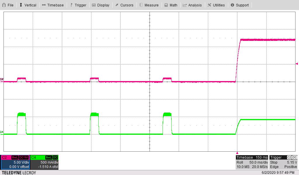
GUID-20200813-CA0I-FLXR-0SWS-4CPT5PJ7BCGM-low.jpgFigure 3-21 Short-Circuit Recovery (VOUT: 5 V/div, IOUT: 500 mA/div, 50 ms/div)