TIDT202 September   2020


  1.   Description
  2. 1Test Prerequisites
    1. 1.1 Design Requirements
    2. 1.2 Required Equipment
    3. 1.3 Dimensions
  3. 2Testing and Results
    1. 2.1 Efficiency Graphs
    2. 2.2 Efficiency Data
    3. 2.3 Load Regulation
    4. 2.4 Thermal Images
  4. 3Waveforms
    1. 3.1 Switching
    2. 3.2 Output Voltage Ripple
    3. 3.3 Load Transients
    4. 3.4 Start-up Sequence
    5. 3.5 Undervoltage Protection
    6. 3.6 Thermal Management

Output Voltage Ripple

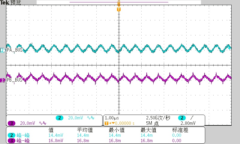
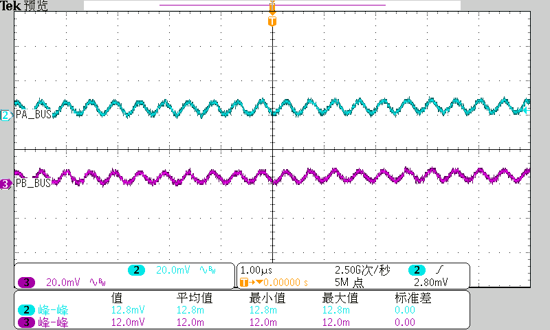
Output voltage ripple is shown in the following figures.
GUID-20200910-CA0I-VPFZ-CH47-MN10L2CSSQC6-low.png

CH2: VPA_BUS

CH3: VPB_BUS
Figure 3-3 13.5V input, 5.17V no-load
GUID-20200910-CA0I-8L5L-J0JK-0QCVXMHQRTJ2-low.png

CH2: VPA_BUS

CH3: VPB_BUS
Figure 3-4 13.5V input, 5.17V full-load