TIDT225 March 2021
4.3 Output Voltage Ripple
Output voltage ripple is shown in the following figures.
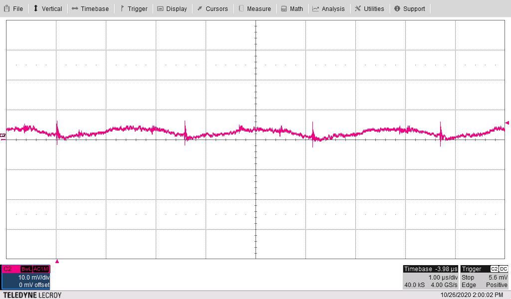 Figure 4-12 18V1 Ripple Voltage With Vin = 12 V and all
Maximum Loads, Bandwidth = 20 MHz
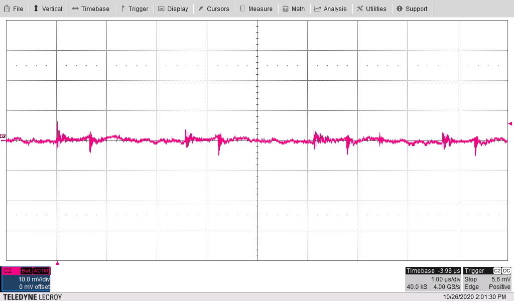 Figure 4-13 –5.1V1 Ripple Voltage With Vin = 12 V and all
Maximum Loads, Bandwidth = 20 MHz
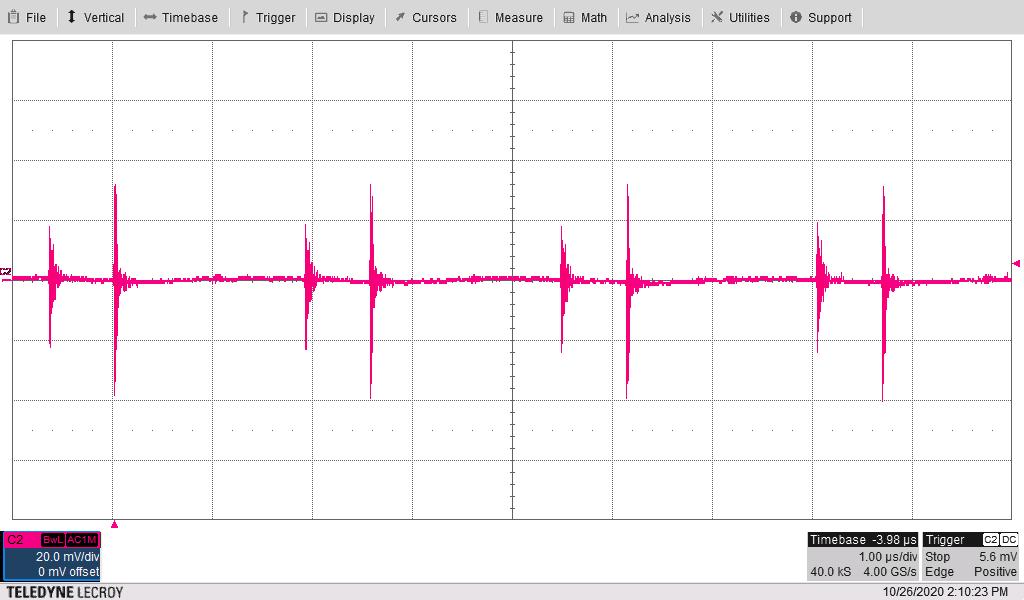 Figure 4-14 18V2 Ripple Voltage With Vin = 12 V and all
Maximum Loads, Bandwidth = 20 MHz
 Figure 4-15 –5.1V2 Ripple Voltage With Vin = 12 V and all
Maximum Loads, Bandwidth = 20 MHz
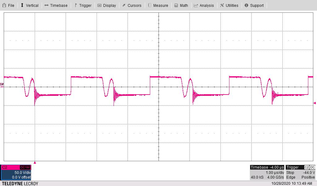 Figure 4-16 Transformer Secondary Switch Node Voltage (T1
– pin 6 and pin 7) With Vin = 7 V and Maximum Loads
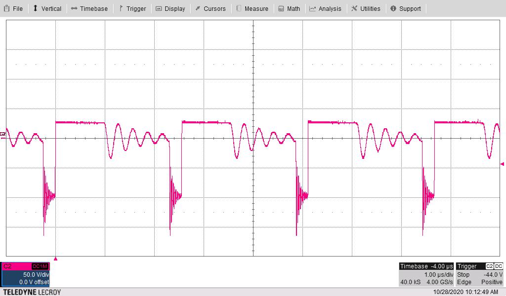 Figure 4-17 Transformer Secondary Switch Node Voltage (T1
– pin 6 and pin 7) With Vin = 32 V and Maximum Loads