TIDT225 March 2021
4.1 Start-up
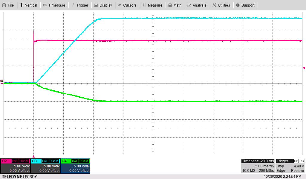
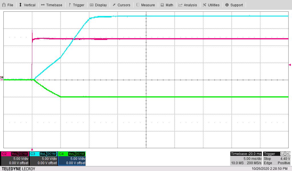
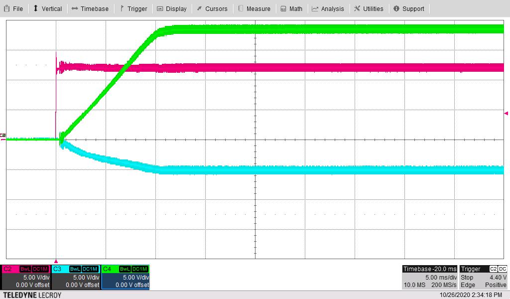
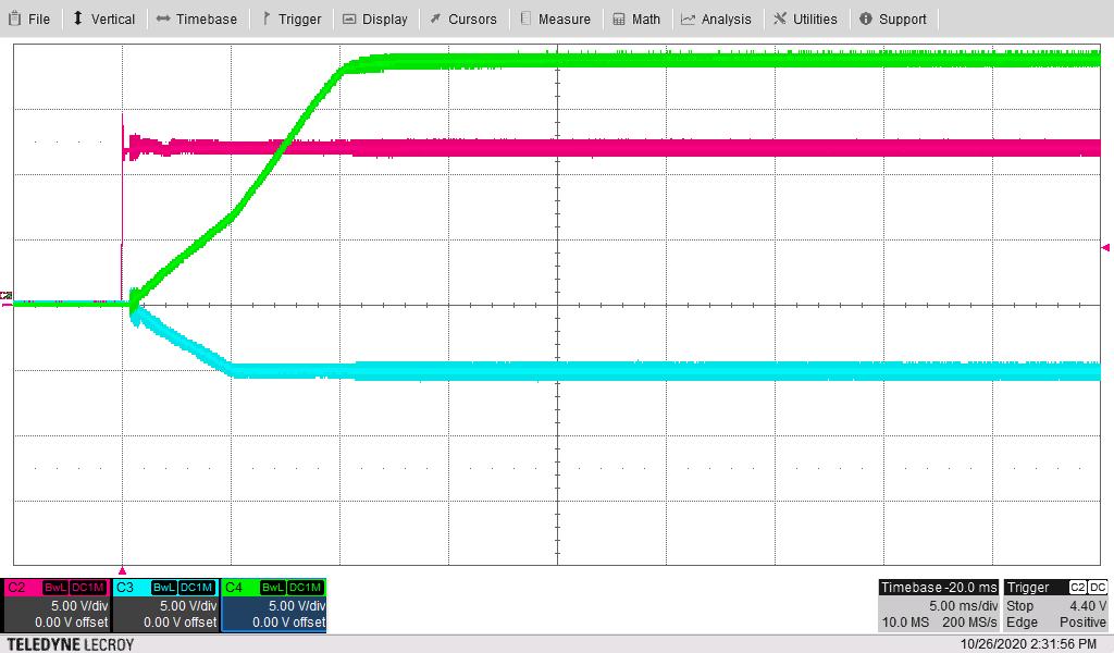
Start-up behavior is shown in the following figures.

All outputs are at max loads
Figure 4-1 Start-up Sequence for +18V1 (Blue)
and –5.1V1 (Green) With Vin = 12 V (Red)
All outputs are unloaded
Figure 4-2 Start-up Sequence for +18V1 (Blue)
and –5.1V1 (Green) With Vin = 12 V (Red)
All outputs are at max loads
Noise on isolated outputs V2, V3, or V4 can be reduced by adding a common-mode capacitor, similar to C26, on each output
Figure 4-3 Start-up Sequence for +18V4 (Blue)
and –5.1V4 (Green) With Vin = 12 V (Red)Noise on isolated outputs V2, V3, or V4 can be reduced by adding a common-mode capacitor, similar to C26, on each output

All outputs are unloaded
Figure 4-4 Start-up Sequence for +18V4 (Blue)
and –5.1V4 (Green) With Vin = 12 V (Red)