TIDT225 March 2021
3.4 Cross Regulation
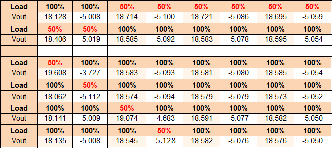
This image shows the output voltage regulation with various 100% and 50% loading combinations with the input voltage set to 12 V.
Voltage regulation is optimally balanced between the +18 V and –5.1V when loaded equally. TI recommends keeping the load imbalance between the +18 V and the –5.1 V to less than 25% to minimize power dissipation in the output Zener diodes.
 Figure 3-6 Output Voltage
Regulation