TIDT225 March 2021
4.2 Switching Waveforms
Switching behavior is shown in the following figures.
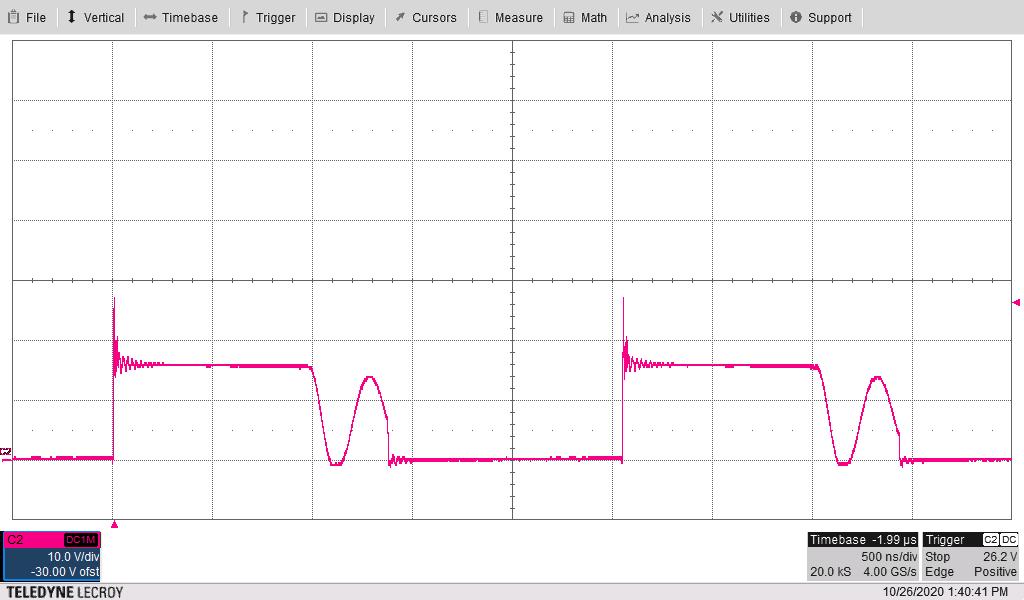 Figure 4-5 FET Switch Node
Voltage at TP3 With Vin = 7 V and Maximum Loads
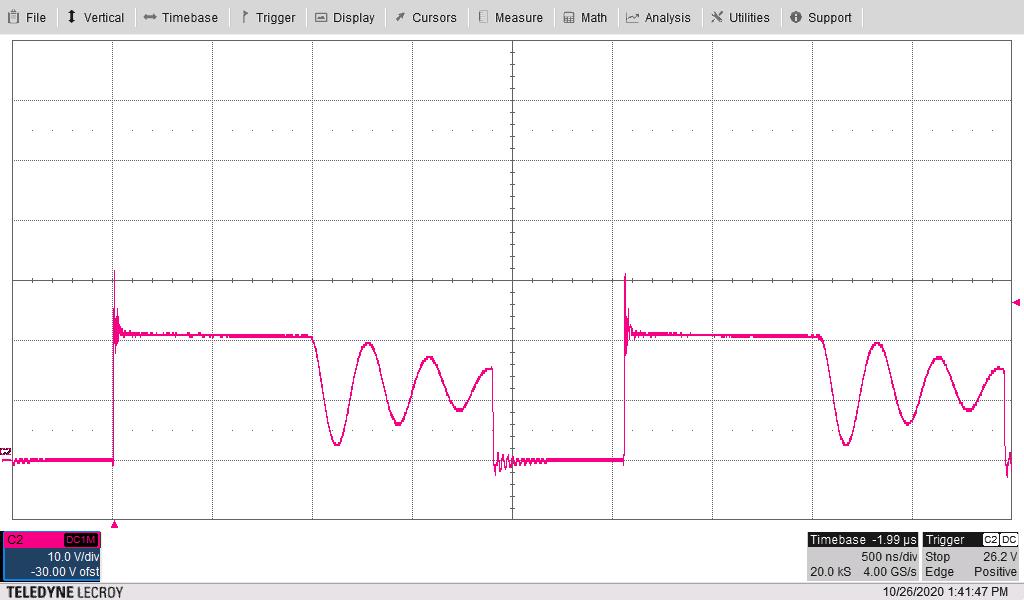 Figure 4-6 FET Switch Node
Voltage at TP3 With Vin = 12 V and Maximum Loads
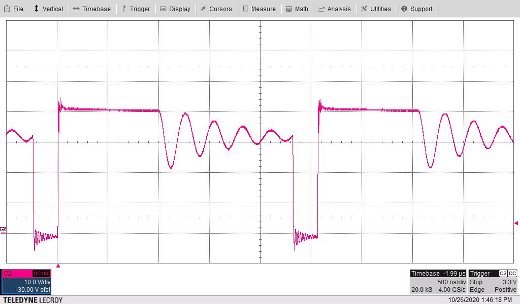 Figure 4-7 FET Switch Node
Voltage at TP3 With Vin = 32 V and Maximum Loads
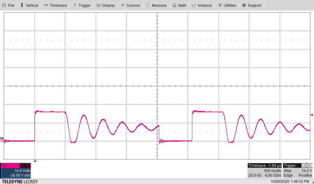 Figure 4-8 FET Switch Node
Voltage at TP3 With Vin = 7 V and no Loads
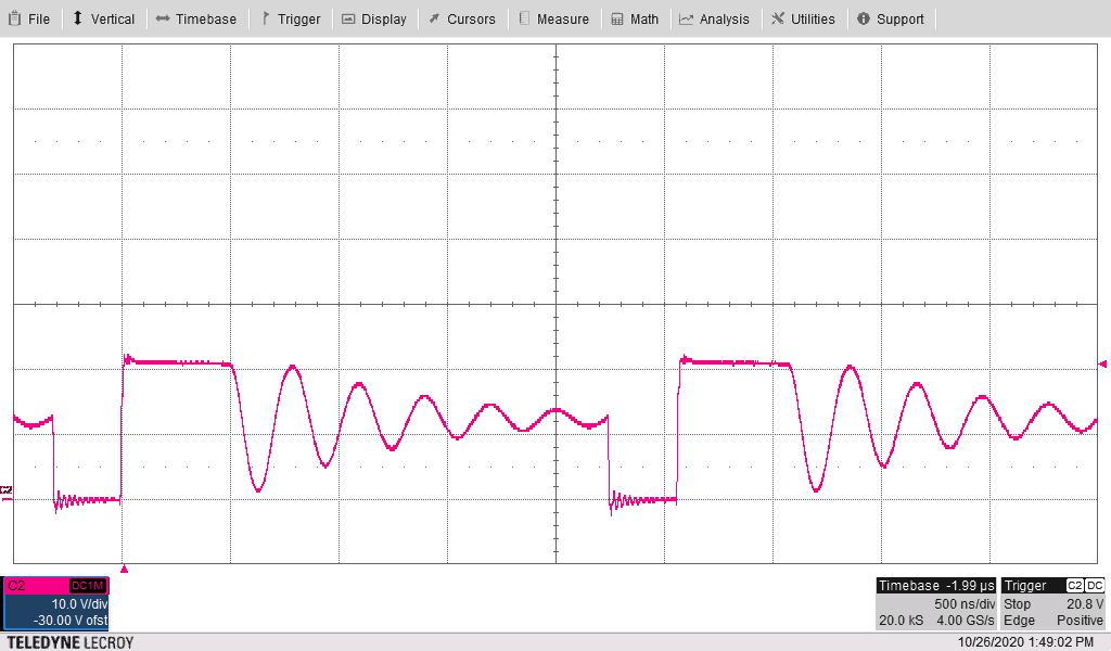 Figure 4-9 FET Switch Node
Voltage at TP3 With Vin = 12 V and no Loads
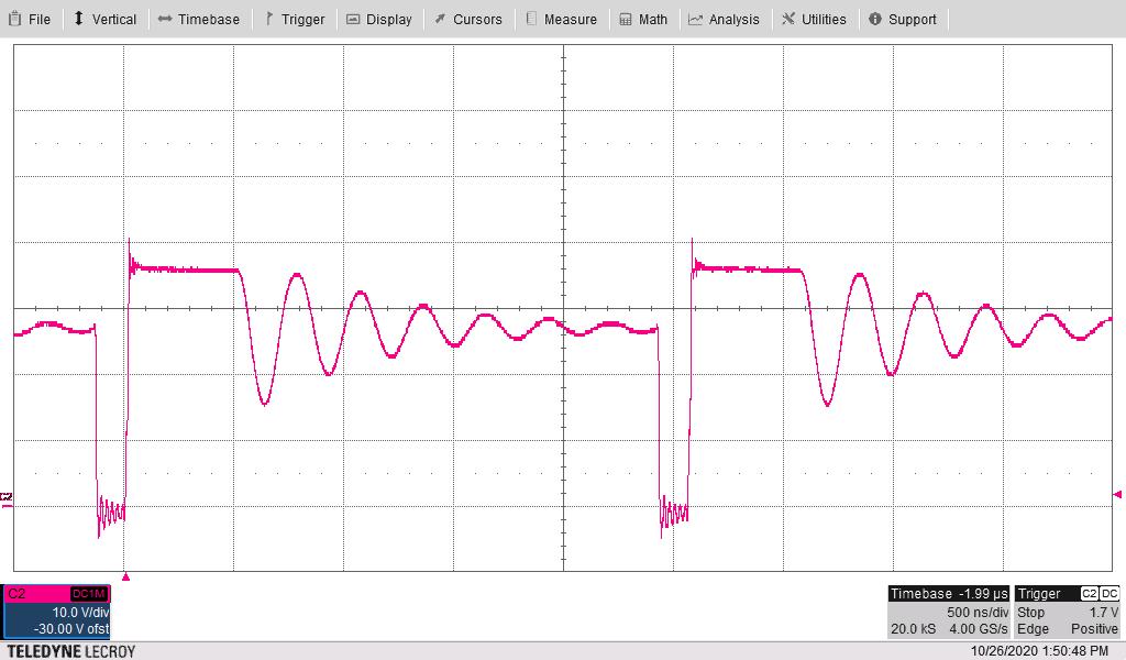 Figure 4-10 FET Switch Node
Voltage at TP3 With Vin = 27 V and no Loads
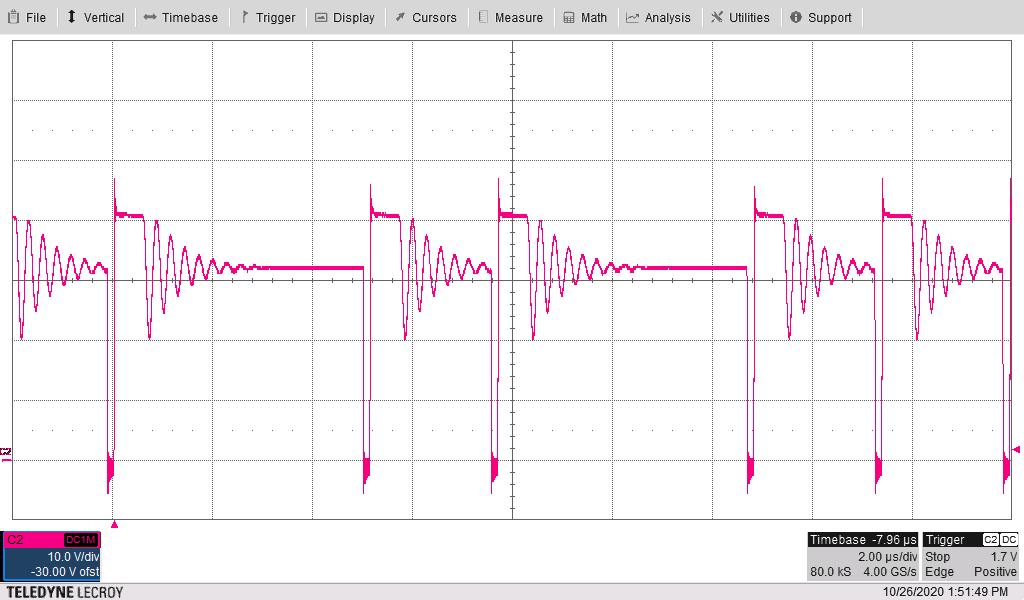 Figure 4-11 FET Switch Node
Voltage at TP3 With Vin = 32 V and no Loads (Note Pulse
Skipping)