TIDT225 March   2021


  1. 1Description
  2. 2Test Prerequisites
    1. 2.1 Voltage and Current Requirements
    2. 2.2 Required Equipment
  3. 3Testing and Results
    1. 3.1 Thermal Images
    2. 3.2 Efficiency and Power Dissipation Graphs
    3. 3.3 Efficiency and Power Dissipation Data
    4. 3.4 Cross Regulation
    5. 3.5 Loop Gain
  4. 4Waveforms
    1. 4.1 Start-up
    2. 4.2 Switching Waveforms
    3. 4.3 Output Voltage Ripple
    4. 4.4 Load Transients

Thermal Images

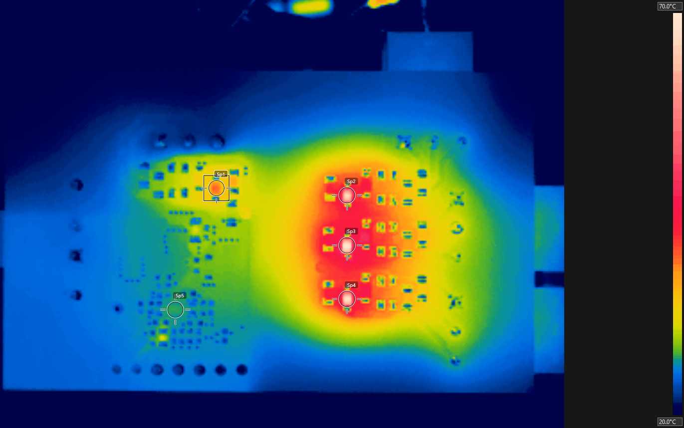
These thermal images show the operating temperature of the top and bottom of the board with 12-V input and all outputs at full load. The images were captured at room temperature after operating for 30 minutes.
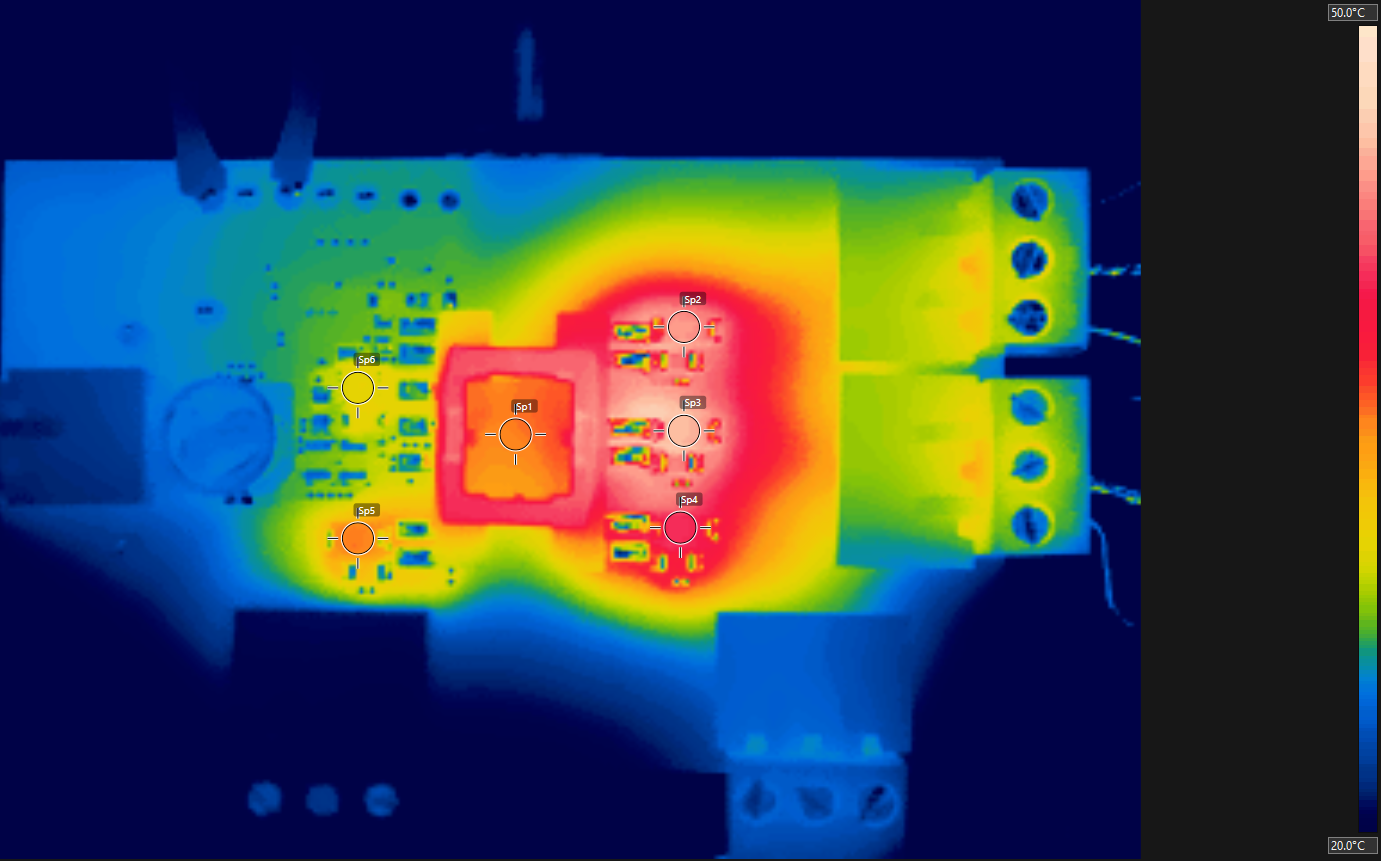
GUID-20210219-CA0I-5B6J-9DD3-NMCCJ7DT2QWV-low.png

Measurement Location Temperature (C)
Sp1 36.3
Sp2 44.8
Sp3 45.9
Sp4 41.4
Sp5 36.3
Sp6 31.8

Figure 3-1 Top Side Thermal Image
GUID-20210219-CA0I-SB3Z-FDSR-RPJNGMJCNHPL-low.png

Measurement Location Temperature (C)
Sp1 42.0
Sp2 67.6
Sp3 70.6
Sp4 69.2
Sp5 28.8

Figure 3-2 Bottom Side Thermal Image