TIDT234 November 2022
3.1 Switching
The following set of figures show the switching waveforms between PFM mode and FPWM mode at 30-V input at no load and 1-A load conditions.
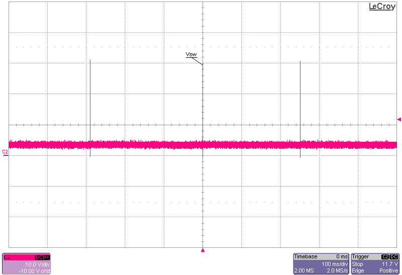 Figure 3-1 Switch Node Voltage, No Load, PFM-Mode
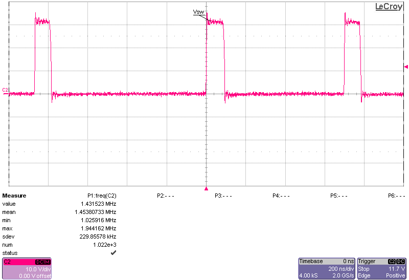 Figure 3-2 Switch Node Voltage, No Load,
FPWM-Mode
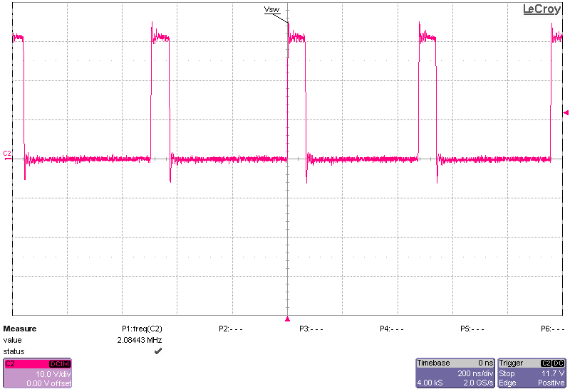 Figure 3-3 Switch Node Voltage, 1-A Load,
PFM-Mode
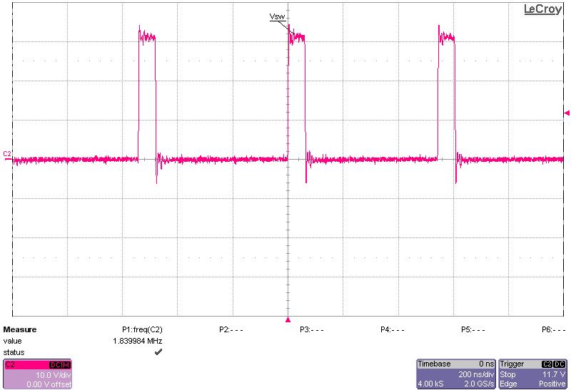 Figure 3-4 Switch Node Voltage, 1-A Load,
FPWM-Mode
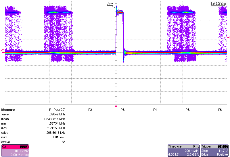 Figure 3-5 Switch Node Voltage, 1-A Load, Displaying
Dither, PFM-Mode
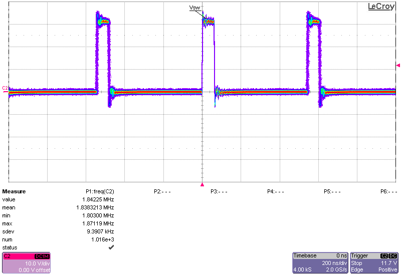 Figure 3-6 Switch Node Voltage, 1-A Load, Displaying
Dither, FPWM-Mode