TIDT236 March 2022 TPS7H1101A-SP
2.3 Thermal Images
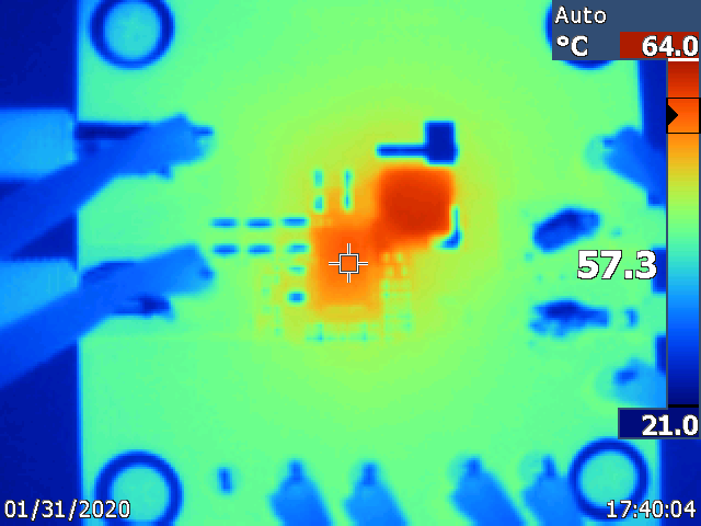
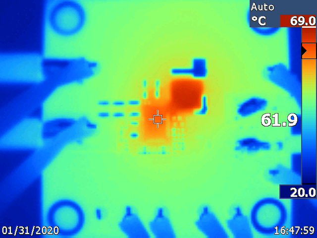
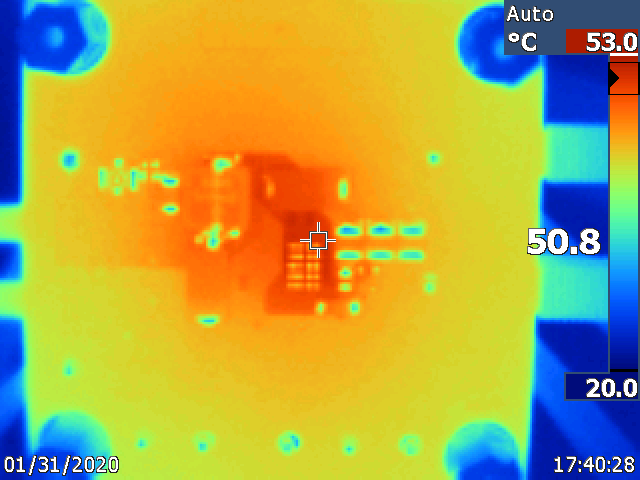
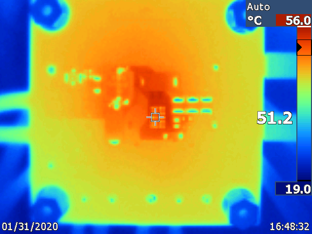
The thermal images in the following figures show operation at 12-V input and –0.2-V and –0.6-V outputs at 15-A load, with no airflow. Thermals images were taken of both the top and bottom side of the board and were captured after the board had reached thermal equilibrium.
 Figure 2-2 Thermal Image, Top Side of
Board, 12-V Input, –0.2-V Output at 15-A Load
 Figure 2-4 Thermal Image, Top Side of
Board, 12-V Input, –0.6-V Output at 15-A Load
 Figure 2-3 Thermal Image, Bottom Side
of Board, 12-V Input, –0.2-V Output at 15-A Load
 Figure 2-5 Thermal Image, Bottom Side
of Board, 12-V Input, –0.6-V Output at 15-A Load