TIDT236 March 2022 TPS7H1101A-SP
1.4 Dimensions
The Top Side and Bottom Side images present the top and bottom photos of the PMP21194 Rev B board. The board dimensions are 2.1 in × 2.1 in (53.3 mm × 53.3 mm). The actual solution size is approximately 0.98 in × 0.72 in (24.9 mm × 18.3 mm).
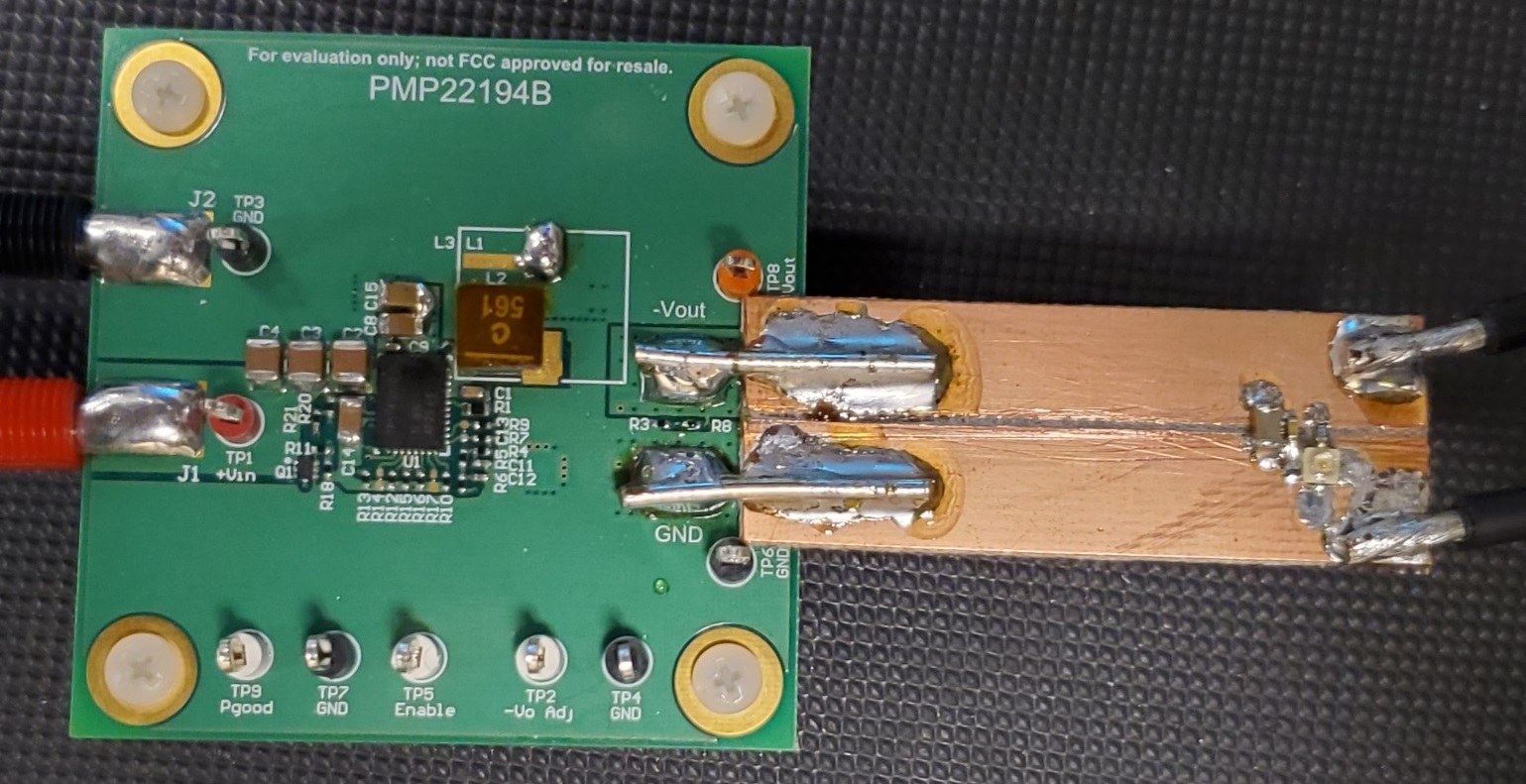
Figure 1-1 presents the top photo of the PMP21194 RevB board with an output extension board connected, to allow for a less noisy output voltage ripple measurement to be made. Since the original placement of the output voltage connector was very close to the switch node, a lot of noise was being injected into the connector which appeared as large, sharp spikes superimposed on the actual output ripple voltage. The addition of this copper clad board allowed for the point of measurement to be physically further from the noise source, that is, switch node.
 Figure 1-1 Top of PMP21194 Board (with
extended output board to take output voltage ripple measurements away from the
switch node, where noise is being coupled into the VOUT connector,
J3)