TIDT244 July 2021
4.5 Voltage Loop to Current Loop Transition
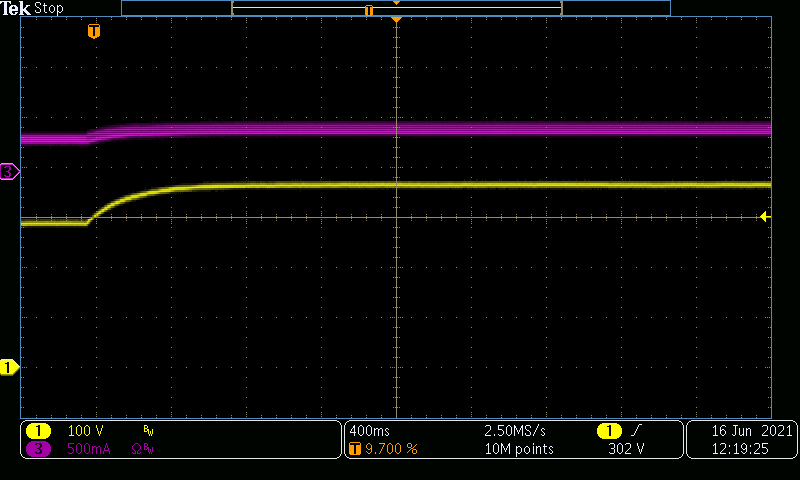
The following figure shows the transition between the voltage loop control mode and the current loop control mode.
In the beginning state, the board is set to 440 mA of output current and 282 V of output voltage. The resistive load is set to 800 Ω. In this state, the load is drawing less current than the 440 mA current limit. This means that the output voltage is regulated at 282 V and the voltage loop is in control.
In the end state, the board output voltage setting is changed from 282 V to 400 V. The current control loop limits the output current to 440 mA and the output voltage is limited to less than 400 V.
 Figure 4-11 VIN = 400 V, IOUT = 0.44 A. Resistive Load = 800 Ω (VOUT: 100 V/DIV, IOUT: 500 mA/DIV, 400 ms/DIV, BWL = 20 MHz)