TIDT244 July 2021
4.1 Start-up
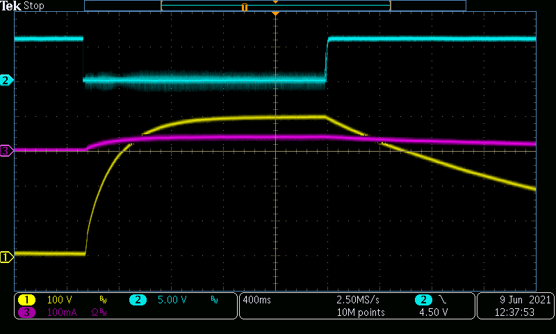
The following figures show the output voltage start-up waveform (YELLOW), the ENABLE waveform (BLUE), and the output current waveform (RED) under two different output conditions.
 Figure 4-1 VIN = 400 V and VOUT =
400 V at 2 A. Resistive Load (VOUT: 100 V/DIV,
ENABLE: 5 V/DIV, IOUT: 2 A/DIV, 400 ms/DIV,
BWL = 20 MHz)
 Figure 4-2 VIN = 400 V and VOUT =
400 V at 40 mA. Resistive Load (VOUT: 100 V/DIV,
ENABLE: 5 V/DIV, IOUT: 100 mA/DIV, 400
ms/DIV, BWL = 20 MHz)