TIDT244 July   2021


  1. 1Description
  2. 2Test Prerequisites
    1. 2.1 Voltage and Current Requirements
    2. 2.2 Required Equipment
  3. 3Testing and Results
    1. 3.1 Thermal Images
    2. 3.2 Efficiency and Power Dissipation Graph
    3. 3.3 Efficiency and Power Dissipation Data
    4. 3.4 Current Regulation
    5. 3.5 Voltage Regulation
  4. 4Waveforms
    1. 4.1 Start-up
    2. 4.2 Switch Node
    3. 4.3 Output Voltage Ripple
    4. 4.4 Current Loop to Voltage Loop Transition
    5. 4.5 Voltage Loop to Current Loop Transition
    6. 4.6 Bias Voltage Start-up
    7. 4.7 Bias Voltage Switch Nodes
    8. 4.8 Output Current Sense Signal

Bias Voltage Start-up

This board uses +18 V (BLUE), +12 V (RED), and –5 V (GREEN) bias rails to operate. The following figure shows the start-up behaviors of the +18 V, –5 V, and EN-drv (YELLOW) signals when the external 12-V bias is applied at J4. The start-up speed of the bias rails is determined by the start-up speed of the external 12-V bias.
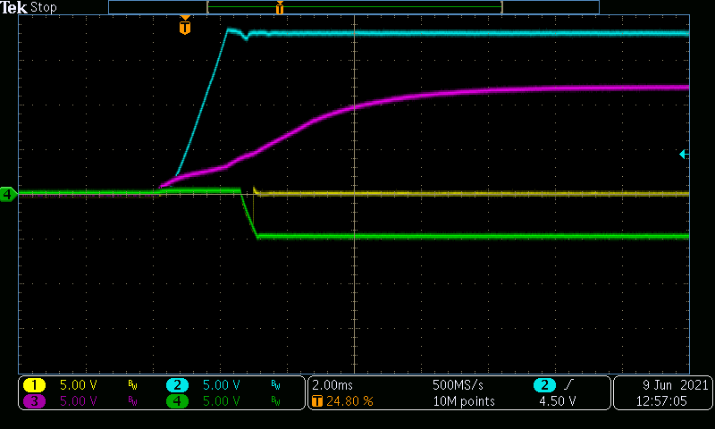
GUID-20210611-CA0I-F1X3-VLXM-GBM8P0X3BVVF-low.pngFigure 4-12 (+18 V: 5 V/DIV, +12 V: 5 V/DIV, –5 V: 5 V/DIV, EN-drv: 5 V/DIV, 200 ms/DIV, BWL = 20 MHz)