TIDT247 February 2022
5 Waveforms
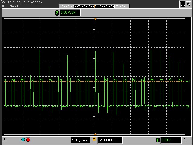
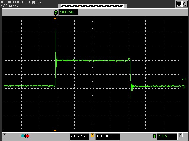
In the switch node waveforms in Figure 5-1 and Figure 5-2, no snubber circuit is installed. These are 0-Ω gate resistor at a switching MOSFET.

Channel 2 – 5 V/div
Figure 5-1 Switch Node - 5 µs/div
Channel 2 – 5 V/div
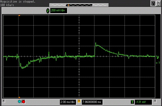
Figure 5-2 Switch Node - 200 ns/divFigure 5-3 shows the load transient waveform.

Channel 2 – output voltage [200 mV/div, 2
ms/div, AC coupled]
Figure 5-3 Load Transient - 1.5 A to 3 A to 1.5
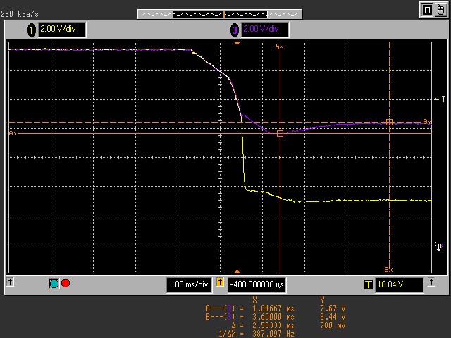
AFigure 5-4 shows the manual input voltage switchover waveform.

Channel 1 – Boost converter VIN [2
V/div, 1 ms/div, DC coupled]
Channel 3 – Boost converter VOUT [2
V/div, 1 ms/div, DC coupled]
Figure 5-4 Manual Input Voltage
Switchover