TIDT249 September 2021
4.1 PFC Waveforms
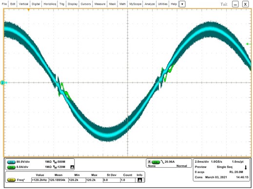
Figure 4-1 shows the PFC input voltage and input current waveform measured at the following parameters:
- Traces
- C2: VIN
- C4: IIN
- Conditions
- VIN = 208 V
- VOUT = 400 V
- ROUT = 43 Ω
 Figure 4-1 PFC Input Voltage and Input Current
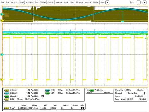
Figure 4-2 shows the PFC GaN drain voltage waveform measured at the following parameters:
- Traces
- C1: GaN Switch Node Drain Voltage
- C2: VIN
- C4: IIN
- Conditions
- VIN = 208 V
- VOUT = 400 V
- ROUT = 43 Ω
 Figure 4-2 PFC GaN Drain Voltage
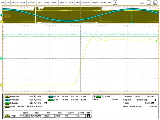
A zoom-in of the GaN switch drain-to-source voltage transition is shown to be approximately 20 ns in Figure 4-3. This rapid transition comes from the low COSS of the LMG3522.
The waveform in Figure 4-3 was measured using the following parameters:
- Traces
- C1: GaN Switch Node Drain Voltage
- C2: VIN
- C4: IIN
- Conditions
- VIN = 208 V
- VOUT = 400 V
- ROUT = 43 Ω
 Figure 4-3 PFC GaN Drain Voltage - Transition