TIDT252 December   2021


  1.   Description
  2.   Features
  3.   Applications
  4. 1Test Prerequisites
    1. 1.1 Voltage and Current Requirements
    2. 1.2 Considerations
    3. 1.3 Dimensions
  5. 2Testing and Results
    1. 2.1 Efficiency Graphs
    2. 2.2 Efficiency Data
    3. 2.3 Thermal Image
    4. 2.4 Bode Plot
  6. 3Waveforms
    1. 3.1 Switching
    2. 3.2 Input Voltage Ripple
    3. 3.3 Output Voltage Ripple
    4. 3.4 Load Transients
    5. 3.5 Start-up Sequence
    6. 3.6 Undervoltage Protection

Switching

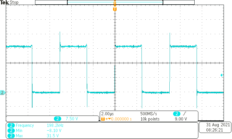
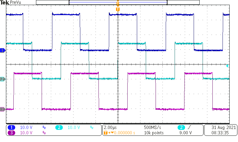
Switching behavior is shown in Figure 3-1 and Figure 3-2.
GUID-20211104-SS0I-ZTGZ-JWRF-JKWDQSNMRPT8-low.png
Ch2: Switching node at 12.0 VIN and 60.0-A load current [scale: 7.50 V/div, 2.0 μs/div], phase 4
Figure 3-1 Switching Single Phase
GUID-20211104-SS0I-9KKB-2KV2-HLHF3WK8Z24X-low.png
Ch1: Switching node at 12.0 VIN and 60.0-A load current [scale: 10.0 V/div, 2.0 μs/div], phase 1
Ch2: Switching node at 12.0 VIN and 60.0-A load current [scale: 10.0 V/div, 2.0 μs/div], phase 2
Ch3: Switching node at 12.0 VIN and 60.0-A load current [scale: 10.0 V/div, 2.0 μs/div], phase 3
Figure 3-2 Switching Multiple Phases