TIDT252 December   2021


  1.   Description
  2.   Features
  3.   Applications
  4. 1Test Prerequisites
    1. 1.1 Voltage and Current Requirements
    2. 1.2 Considerations
    3. 1.3 Dimensions
  5. 2Testing and Results
    1. 2.1 Efficiency Graphs
    2. 2.2 Efficiency Data
    3. 2.3 Thermal Image
    4. 2.4 Bode Plot
  6. 3Waveforms
    1. 3.1 Switching
    2. 3.2 Input Voltage Ripple
    3. 3.3 Output Voltage Ripple
    4. 3.4 Load Transients
    5. 3.5 Start-up Sequence
    6. 3.6 Undervoltage Protection

Input Voltage Ripple

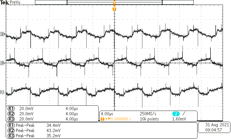
Figure 3-3 shows the input voltage ripple at 9.0 V, 12.0 V, and 16.0 V for a load current of 60.0 A.
GUID-20211104-SS0I-GDLV-VCK9-5X7VPS6VRPVG-low.png
R1: 9.0 VIN, 60.0-A load, 34.4-mV peak-peak-ripple [scale: 20 mV/div, 4.0 μs/div]
R2: 12.0 VIN, 60.0-A load, 43.2-mV peak-peak-ripple [scale: 20 mV/div, 4.0 μs/div]
R3: 16.0 VIN, 60.0-A load, 35.2-mV peak-peak-ripple [scale: 20 mV/div, 4.0 μs/div]
Figure 3-3 Input Voltage Ripple