TIDT257A February   2022  – October 2022


  1.   Description
  2.   Features
  3.   Application
  4. 1Test Prerequisites
    1. 1.1 Voltage and Current Requirements
    2. 1.2 Considerations
    3. 1.3 Dimensions
  5. 2Testing and Results
    1. 2.1 Efficiency Graphs
    2. 2.2 Efficiency Data
      1. 2.2.1 THD Optimization
    3. 2.3 Thermal Images
      1. 2.3.1 Low-Side GaN Junction Temperature
    4. 2.4 Thermal Mechanical Design
      1. 2.4.1 Design Parameters
      2. 2.4.2 Thermal Resistance Calculation
      3. 2.4.3 Heat-Sink Diagrams
    5. 2.5 EMI
  6. 3Waveforms
    1. 3.1 AC Drop
    2. 3.2 Load Transients
    3. 3.3 Start-Up Sequence

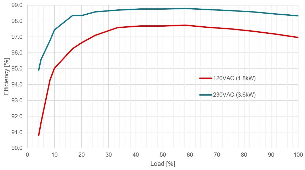
Efficiency Graphs

Conditions

  • Frequency: 65 kHz
  • GaN Slew Rate: 100 V/ns
  • Output: 380 V
  • PFC Inductor: PAL6585.254NL
  • Power analyzer: WT3000E
  • Relay and BB bypass FETs shorted
  • Auxiliary supply not included
GUID-20220217-SS0I-5XTF-KZR9-BCBKBSZHWMSZ-low.jpg Figure 2-1 Efficiency Graph