TIDT259 March 2022
3.1 Switching
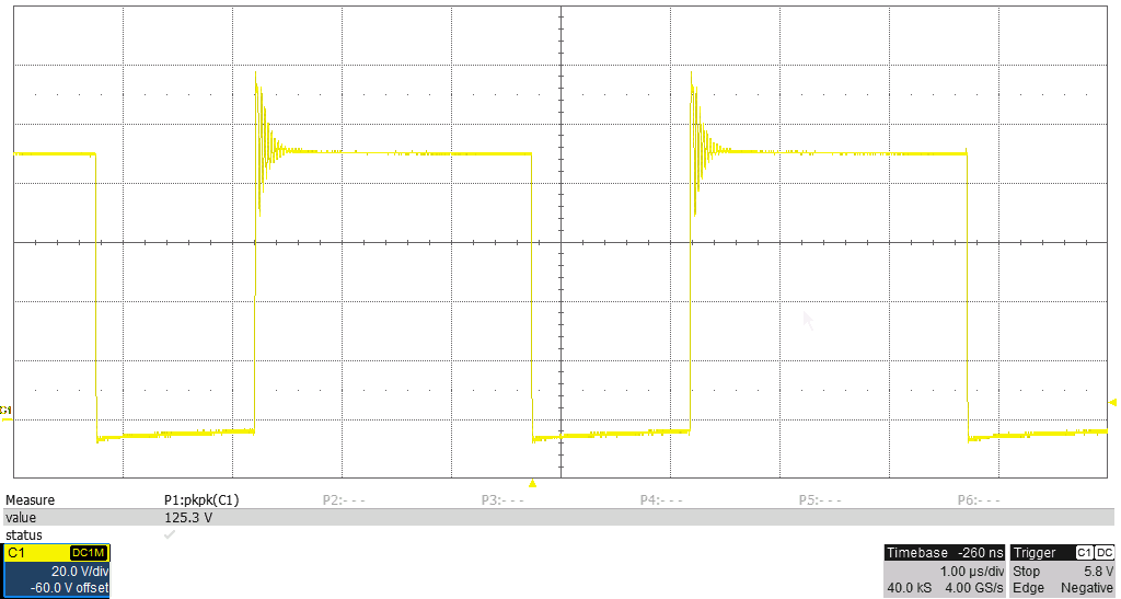
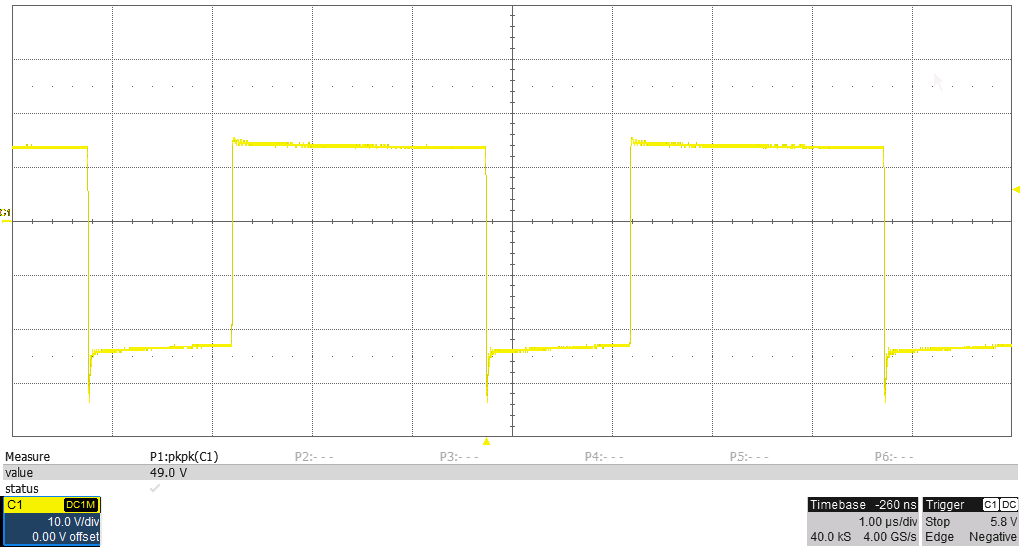
The following images show the switching waveforms.
 Figure 3-1 VDS, Q6, 57-V Input, 3.8-A Load, 20
V/div, 1 μs/div, Measured 125.3 V
 Figure 3-2 Anode-to-Cathode Voltage, D11, 57-V
Input, 3.8-A Load, 10 V/div, 1 μs/div, Measured 49.0 V