TIDT259 March 2022
3.4 Load Transients
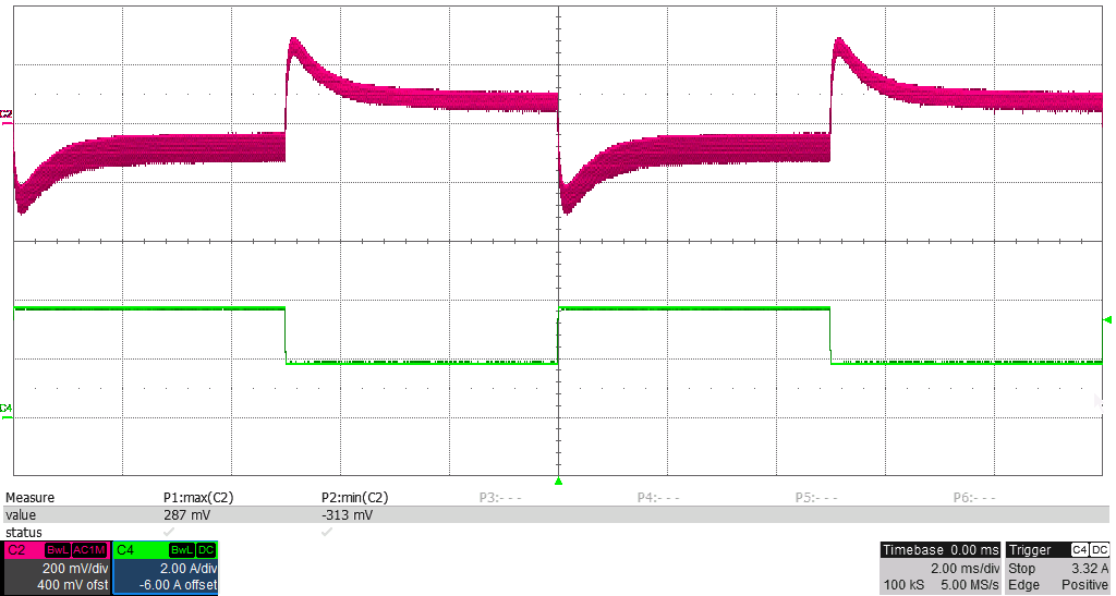
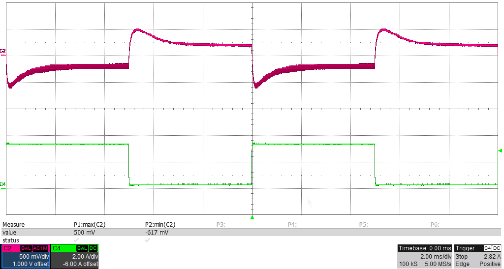
Load transient response is shown in the following figures.
 Figure 3-9 Output Load Step Response, 1.9-A to 3.8-A Load Step (50 to 100%), 200 mV/div, 2 A/div,
2 ms/div, Slew Rate = 250 mA/μs, Measured –313 mV, +287 mV
 Figure 3-10 Output Load Step Response, 380-mA to 3.4-A Load Step (10 to 90%), 500 mV/div, 2 A/div,
2 ms/div, Slew Rate = 250 mA/μs, Measured –617 mV, +500 mV
 Figure 3-11 Output Load Step Response, 1.1-A to 2.6-A Load Step (30 to 70%), 200 mV/div, 2 A/div,
2 ms/div, Slew Rate = 250 mA/μs, Measured –267 mV, +240 mV