TIDT269 April 2022
3.3 Output Load Transients
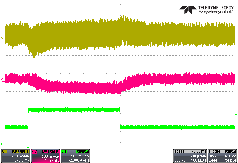
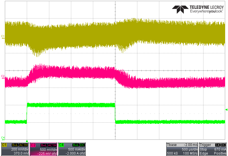
Load transient responses are shown in the following figures.
 Figure 3-6 0.5-A to 1-A Step on +15 V,
95-VDC input, –15 V Loaded With 0.5 A; +15 V on Ch1, –15 V on Ch2, +15-V Load
Current on Ch4
 Figure 3-7 0.5-A to 1-A Step on –15 V,
95-VDC Input, +15 V Loaded With 0.5 A; +15 V on Ch1, –15 V on Ch2, –15-V Load
Current on Ch4