TIDT269 April   2022


  1.   Description
  2.   Features
  3.   Applications
  4. 1Test Prerequisites
    1. 1.1 Input and Output Specifications
    2. 1.2 Dimensions
  5. 2Testing and Results
    1. 2.1 Efficiency Graphs
    2. 2.2 Efficiency Data
    3. 2.3 Output Voltage Cross Regulation
    4. 2.4 Thermal Images
    5. 2.5 Loop Response
  6. 3Waveforms
    1. 3.1 Switching
    2. 3.2 Output Voltage Ripple
    3. 3.3 Output Load Transients

Output Voltage Ripple

Output voltage ripple is shown in the following figures.

GUID-20220321-SS0I-H12Q-FRWB-ZHHSVMBBSXVP-low.png Figure 3-3 70-VDC Input, +15 V on Ch1, –15 V on Ch2
GUID-20220321-SS0I-QTLD-HGTH-NJN71WKMQCSF-low.jpg Figure 3-4 95-VDC Input, +15 V on Ch1, –15 V on Ch2
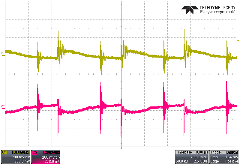
GUID-20220321-SS0I-H4NH-BVBC-PTTWXLHVZL6L-low.png Figure 3-5 120-VDC Input, +15 V on Ch1, –15 V on Ch2