TIDT269 April 2022
2.4 Thermal Images
All images captured with the DUT at 25ºC ambient,
after a 30-minute warm up. The output was loaded with
40 W.
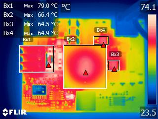 Figure 2-4 70-VDC Input
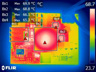 Figure 2-6 120-VDC Input
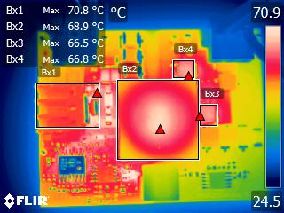 Figure 2-5 95-VDC Input
TIDT269 April 2022
All images captured with the DUT at 25ºC ambient,
after a 30-minute warm up. The output was loaded with
40 W.
 Figure 2-4 70-VDC Input
 Figure 2-6 120-VDC Input
 Figure 2-5 95-VDC Input