TIDT287 August 2022
3.1 Switching
The PMP23123 waveforms are illustrated in the following images.
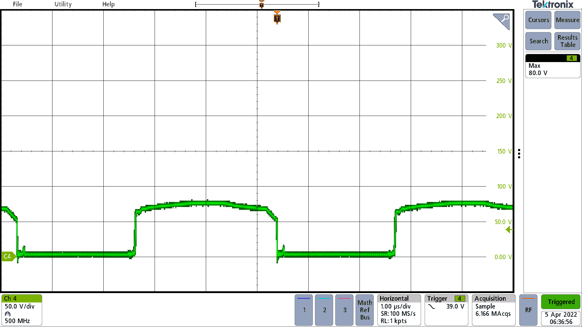 Figure 3-1 Voltage Anode To Cathode, D4, 24-V Input,
40-V, 2.5-A Output, 50 V/div, 1 μs/div, Measured 80-V Peak
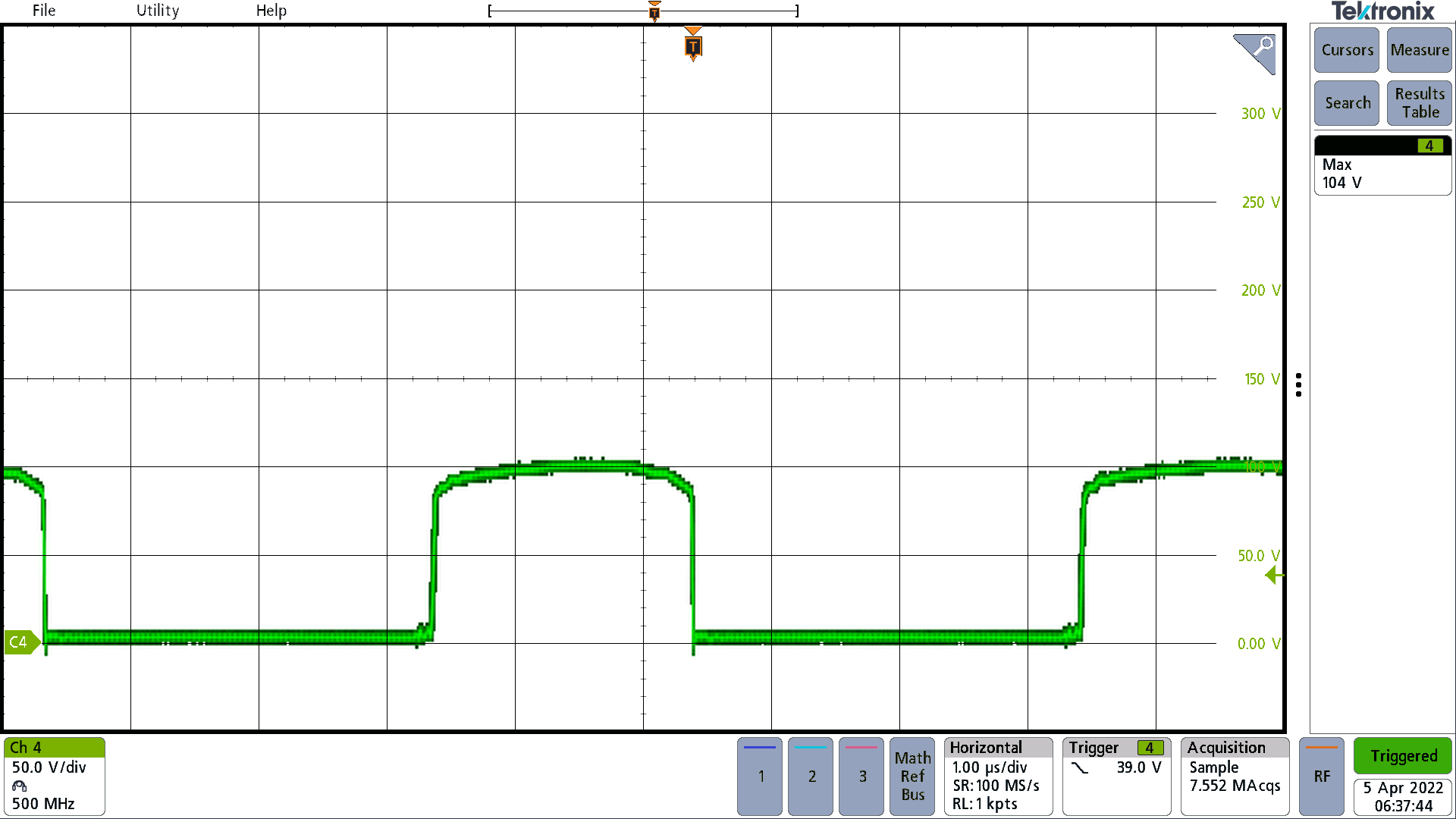 Figure 3-3 Voltage Anode to Cathode, D4, 18-V Input,
40-V, 2.5-A Output, 50 V/div, 1 μs/div, Measured 104-V Peak
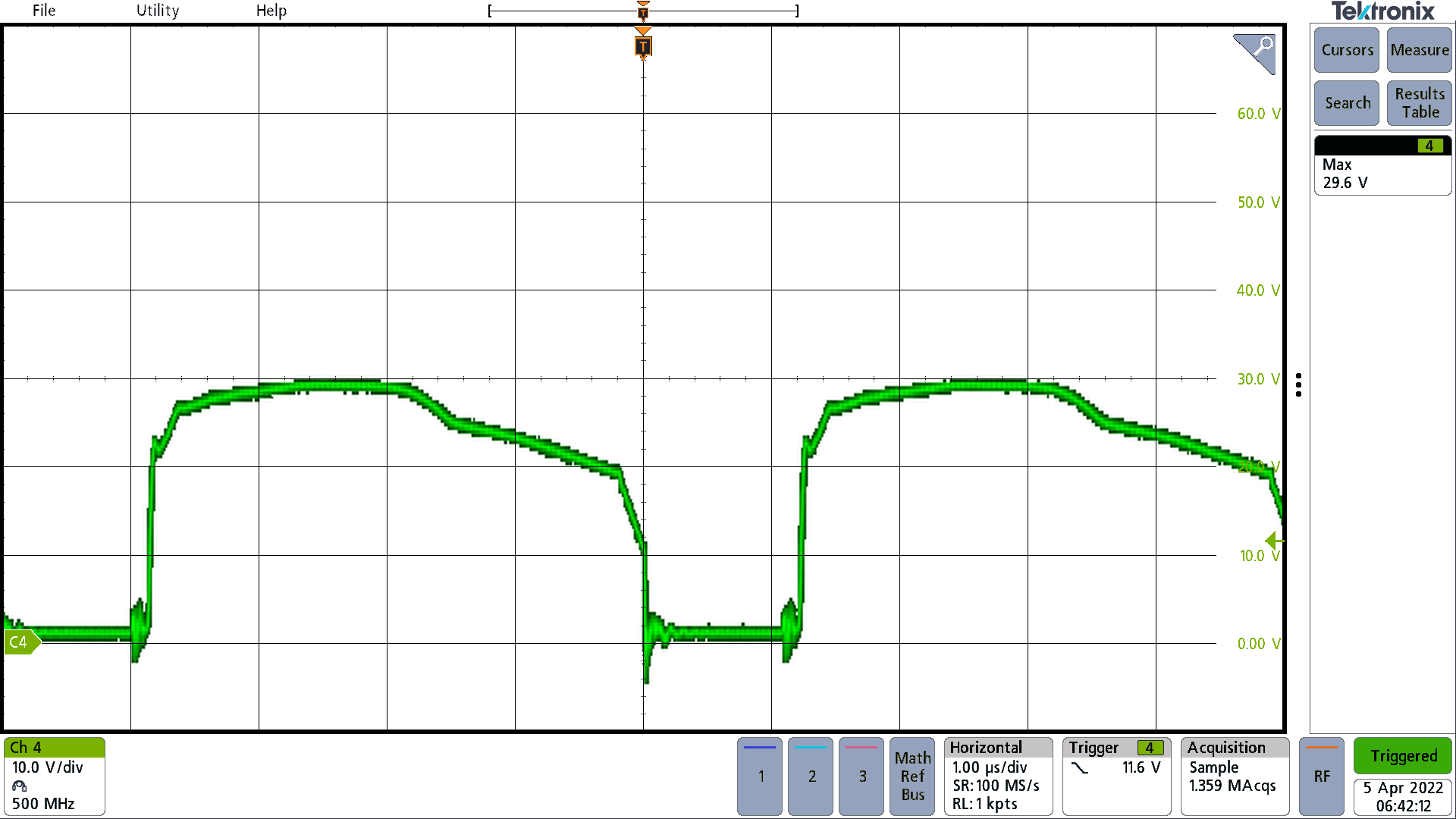 Figure 3-5 Voltage Anode to Cathode, D4, 24-V Input,
19-V, 4-A Output, 10 V/div, 1 μs/div, Measured 29.6-V Peak
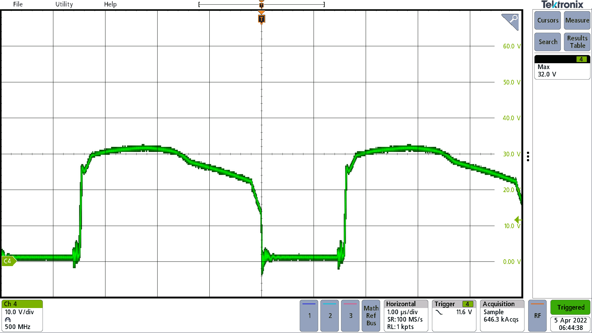 Figure 3-7 Voltage Anode to Cathode, D4, 18-V Input,
19-V, 4-A Output, 10 V/div, 1 μs/div, Measured 32.8-V Peak
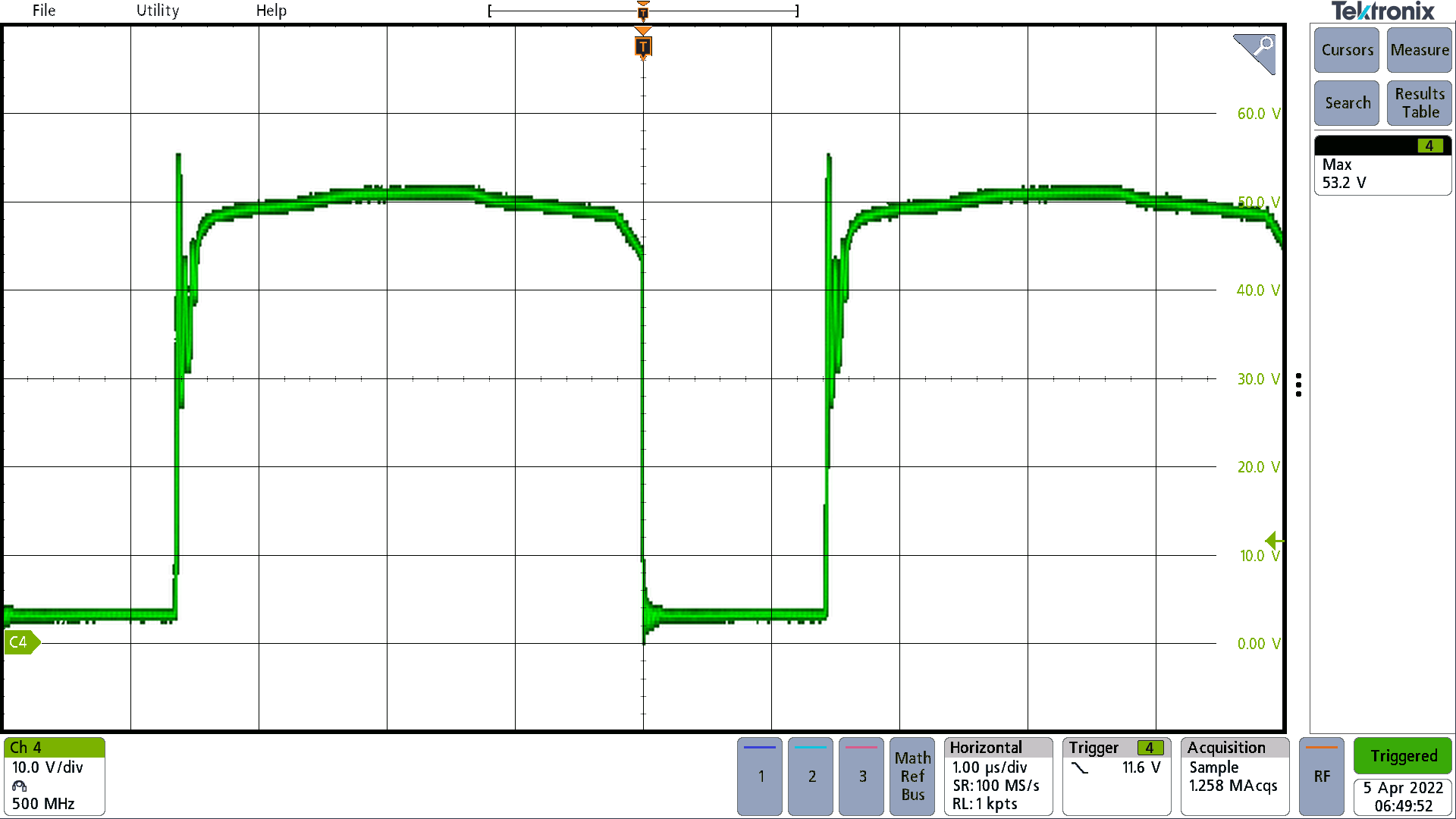 Figure 3-9 Voltage Drain to Source, Q4 and Q6, 36-V
Input, 40-V, 2.5-A Output, 10 V/div, 1 μs/div, Measured 53.2-V Peak
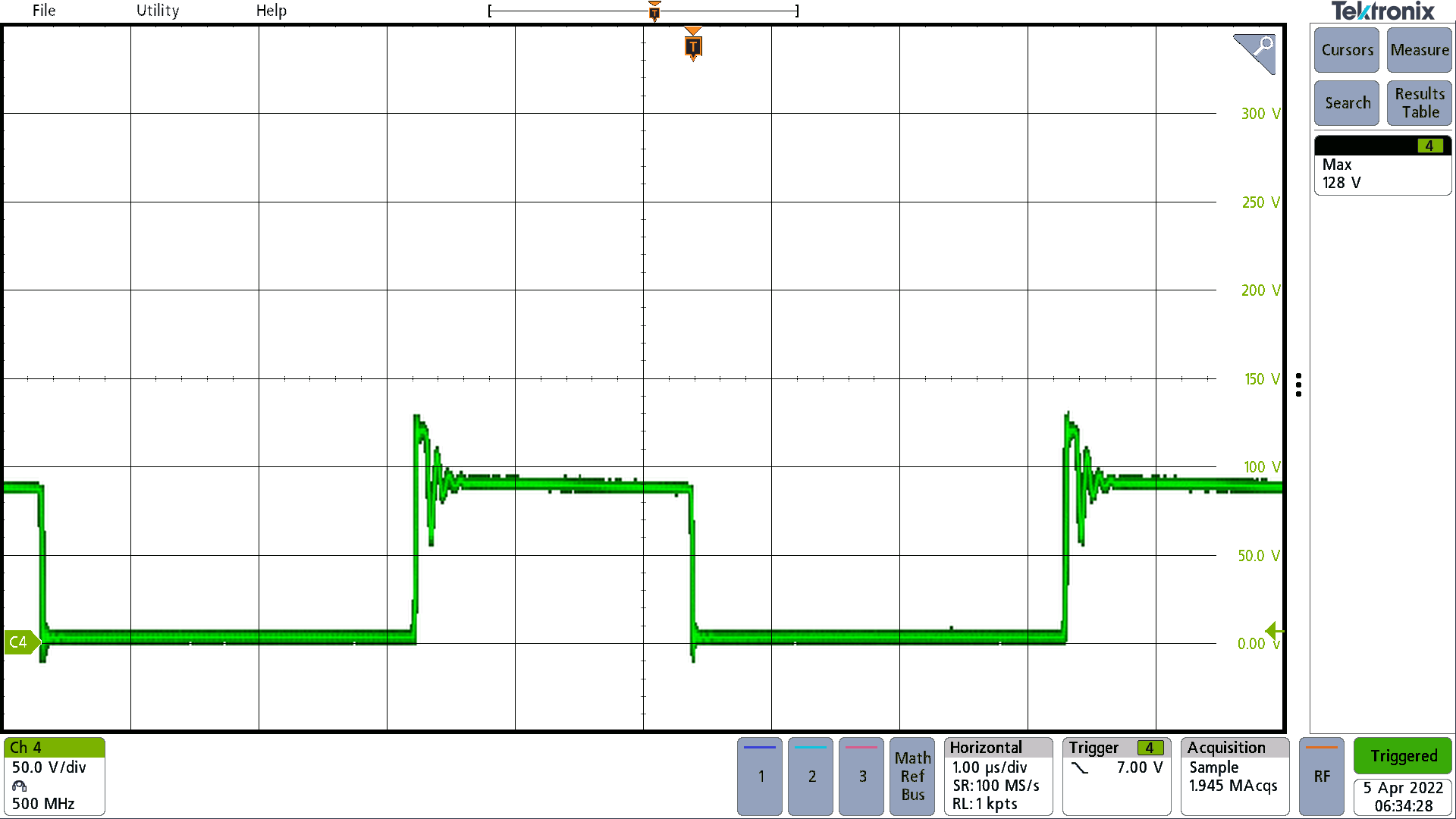 Figure 3-2 Voltage Anode to Cathode, D10, 24-V Input,
40-V, 2.5-A Output, 50 V/div, 1 μs/div, Measured 128-V Peak
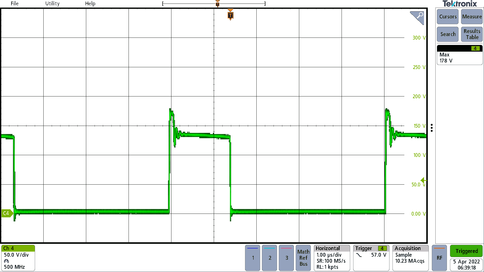 Figure 3-4 Voltage Anode to Cathode, D10, 36-V Input,
40-V, 2.5-A Output, 50 V/div, 1 μs/div, Measured 178-V Peak
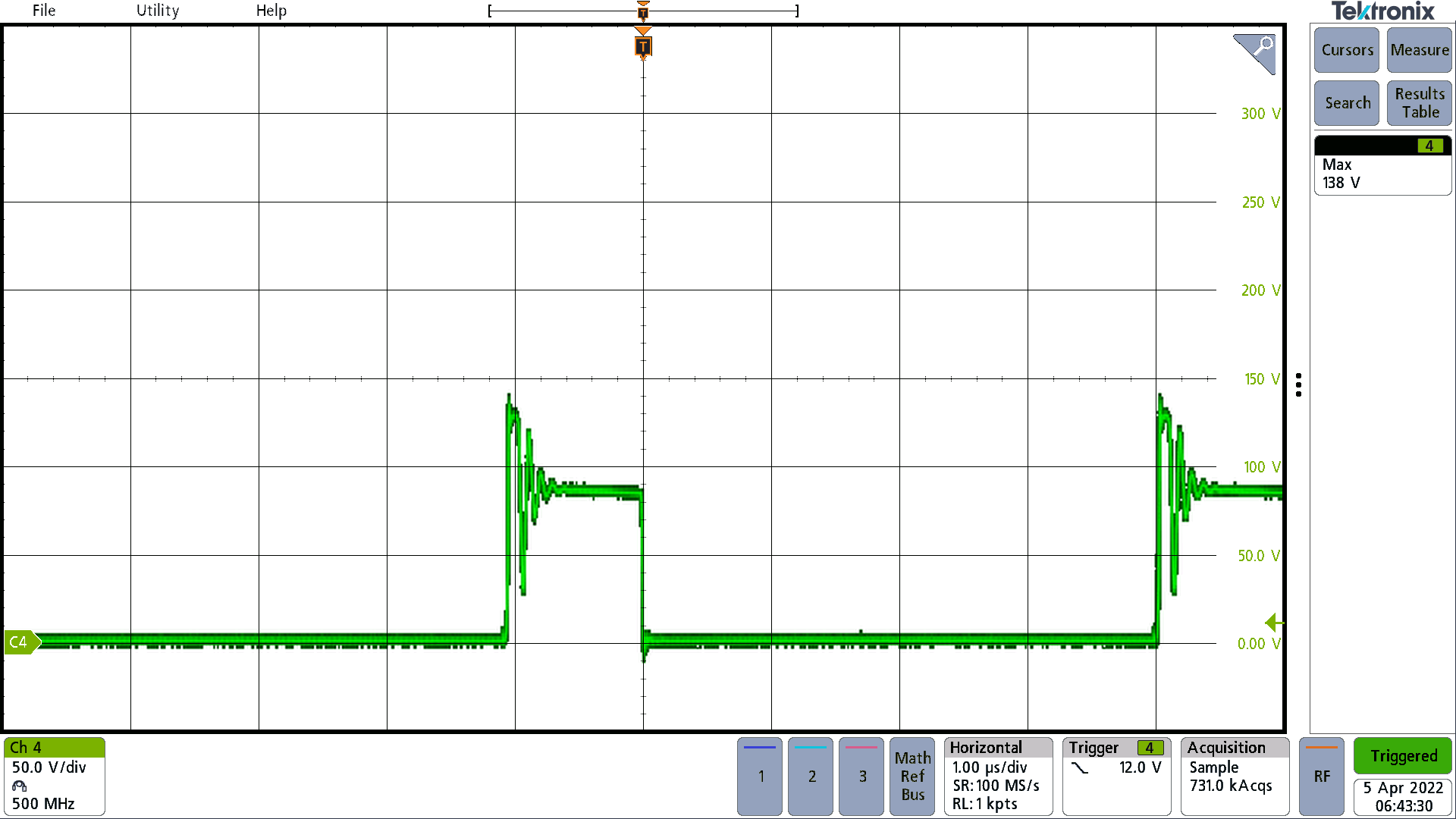 Figure 3-6 Voltage Anode to Cathode, D10, 24-V Input,
19-V, 4-A Output, 50 V/div, 1 μs/div, Measured 138-V Peak
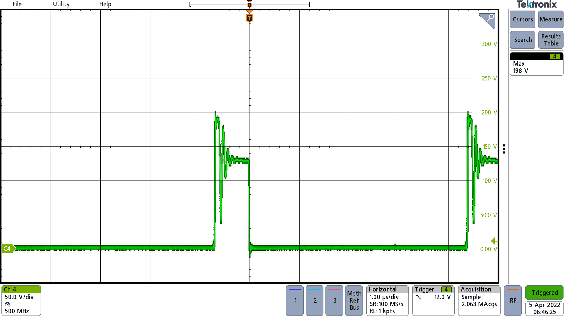 Figure 3-8 Voltage Anode to Cathode, D10, 36-V Input,
19-V, 4-A Output, 50 V/div, 1 μs/div, Measured 198-V Peak
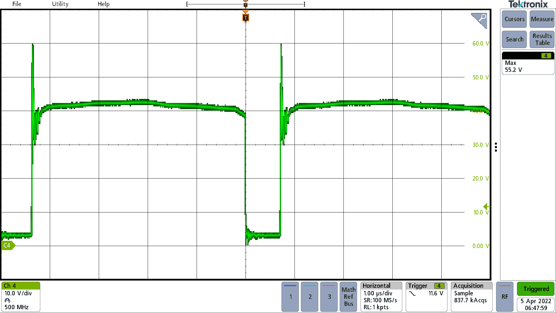 Figure 3-10 Voltage Drain to Source, Q4 and Q6, 36-V
Input, 19-V, 4-A Output, 10 V/div, 1 μs/div, Measured 55.2-V Peak