TIDT287 August 2022
3.5 Output Voltage Step
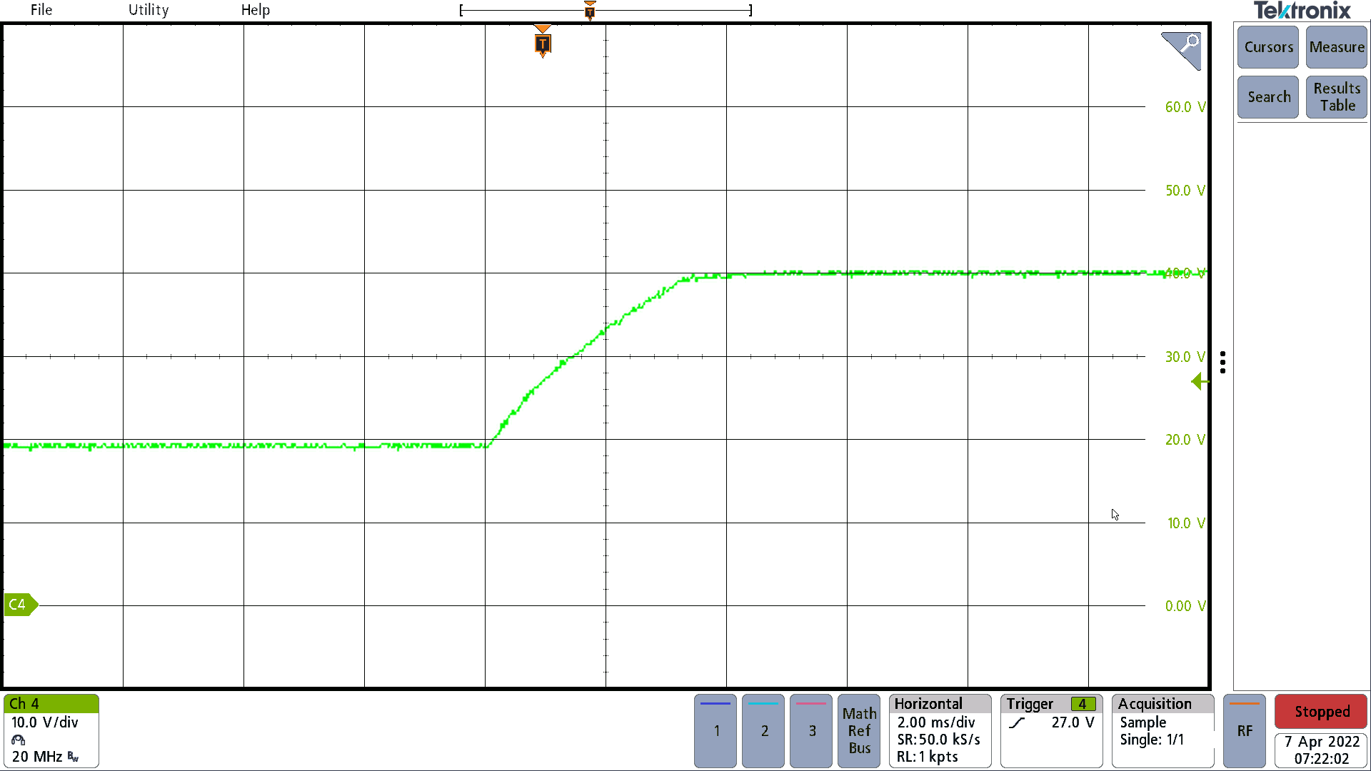
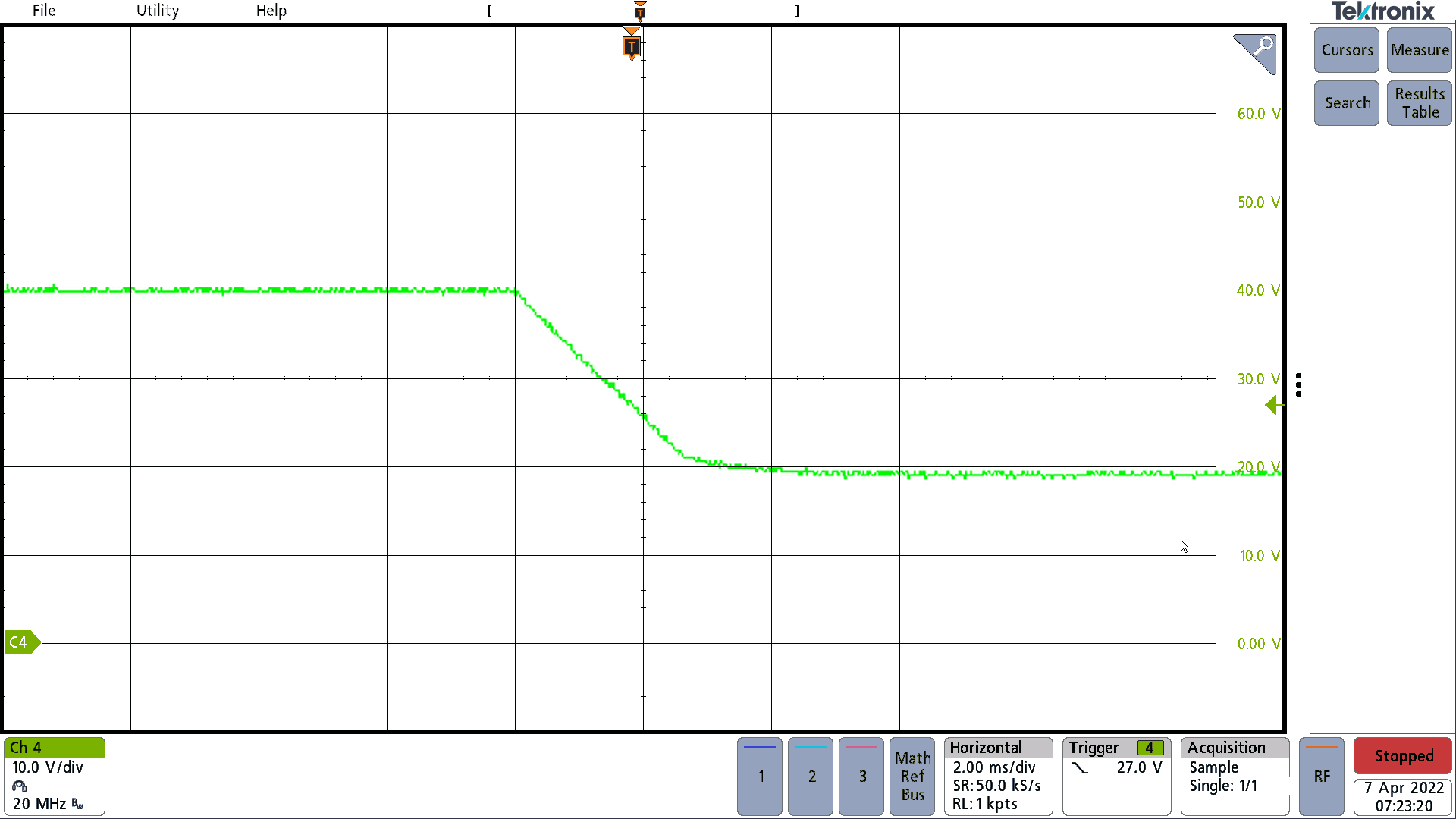
The following images illustrate the PMP23123 output voltage step waveforms.
Tie J3 pin 1 and J4 pin 1 together. Short and open the J3 and J4 pin, 1. 24-V input. A 2.5-A load is at both the 19-V and 40-V output.
 Figure 3-27 19-V to 40-V Output Voltage Transition, 10
V/div, 2 ms/div
 Figure 3-28 40-V to 19-V Output Voltage Transition. 10
V/div, 2 ms/div