TIDT294 June 2022
3.1 Switching Waveforms
Switching behavior is shown in the following figures. Test conditions for these waveforms occur at:
- VIN: 230 V
- VOUT: 400 V
- IOUT: 10 A
Note: Several operating points are illustrated to demonstrate the topology and controls ability to maintain ZVS when the input voltage is both above and below ½ VOUT.
- CH1 - VSW Phase 1
- CH2 - VSW Phase 2
- CH2 - ISW Phase 1
- CH4 - ISW Phase 2
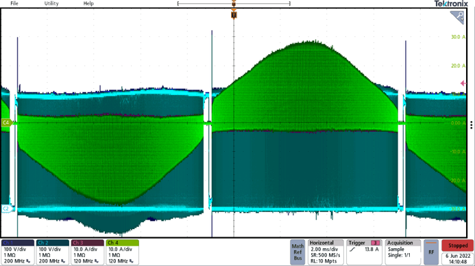 Figure 3-1 Entire Waveform
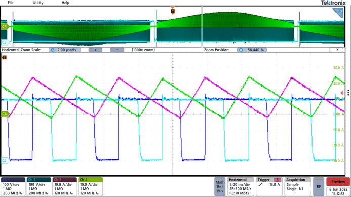 Figure 3-3 VIN > ½ VOUT
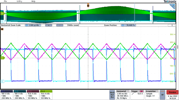 Figure 3-5 VIN = ½ VOUT
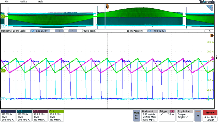 Figure 3-2 VIN < ½ VOUT
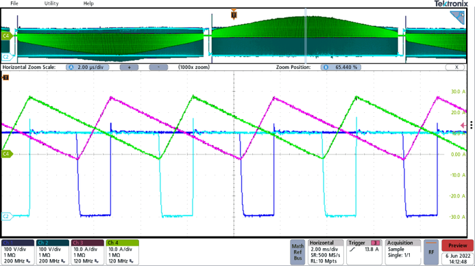 Figure 3-4 VIN > ½ VOUT
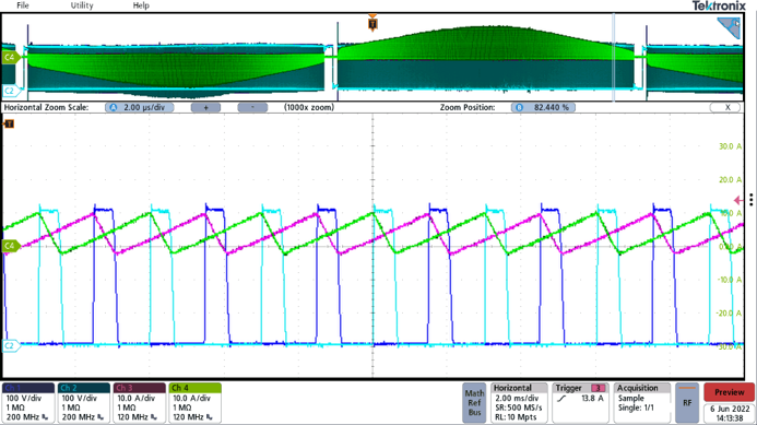 Figure 3-6 VIN < ½ VOUT