TIDT295 August 2022
3.4 Switching Node
Switching node on SW1 and SW2 is shown in the following figures. The waveform channel key is as follows: Pink: SW1-VBUS, Light blue: SW2-VBAT
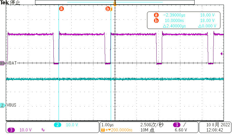 Figure 3-17 19 VBAT to 20 V, 3 A Full Load OTG Mode Working at Boost Mode
 Figure 3-19 21 VBAT to 20 V, 3 A Full Load OTG Mode Working at Buck Mode
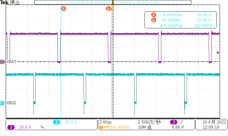 Figure 3-18 20 VBAT to 20 V, 3 A Full Load OTG Mode Working at Buck-Boost Mode
The following images illustrate charging mode switching node.
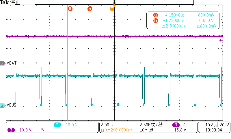 Figure 3-20 20 VBUS to VBAT 21 V Charge Mode Working at Boost Mode
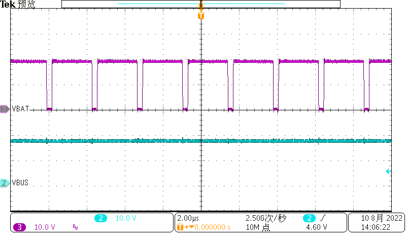 Figure 3-22 20 VBUS to VBAT 19-V Charge Mode Working at Buck Mode
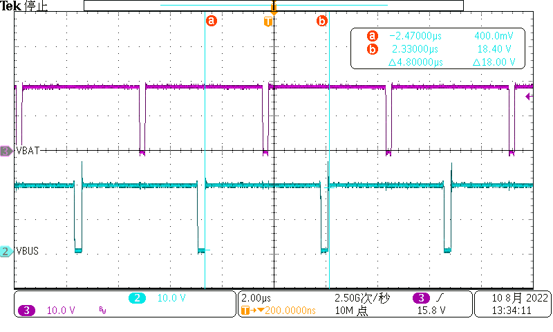 Figure 3-21 20 VBUS to VBAT 20 V Charge Mode Working at Buck-Boost Mode