TIDT295 August 2022
3.3 Load Dynamic
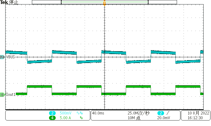
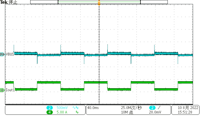
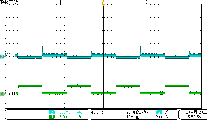
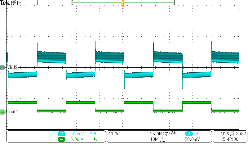
Load dynamic is performed with load dynamic from 0.1 A to 3 A with 2 A/μs slew rate. The output voltage at the PCB board end is recorded for reference.
 Figure 3-13 VBAT 18 V to 5 VBUS 0.1
A to 3 A Load Dynamic
 Figure 3-15 VBAT 18 V to 15 VBUS 0.1
A to 3 A Load Dynamic
 Figure 3-14 VBAT 18 V to 9 VBUS 0.1
A to 3 A Load Dynamic
 Figure 3-16 VBAT 18 V to 20 VBUS 0.1
A to 3 A Load Dynamic