TIDT296 September 2022
3.7 Diode Voltage Stress
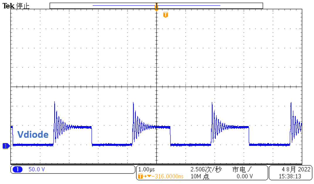
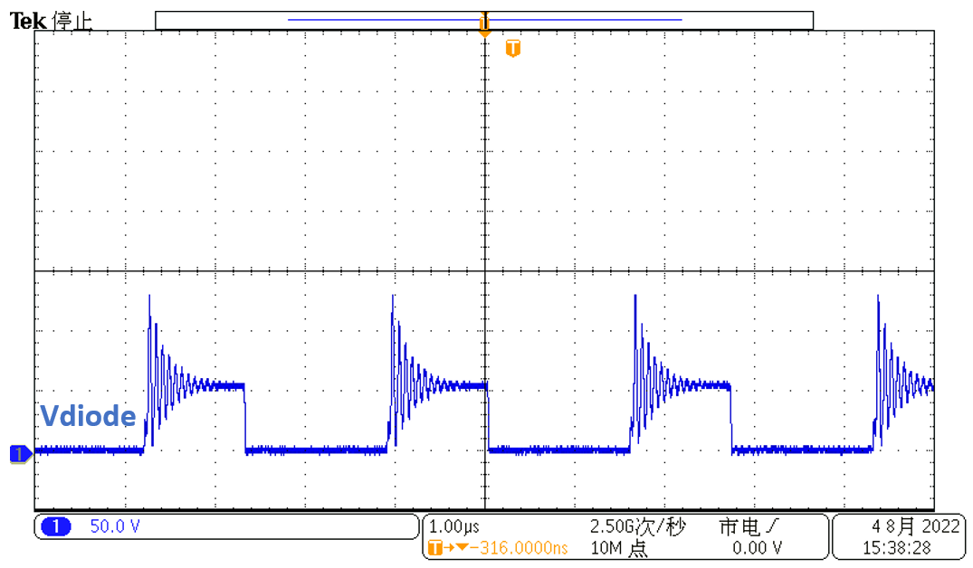
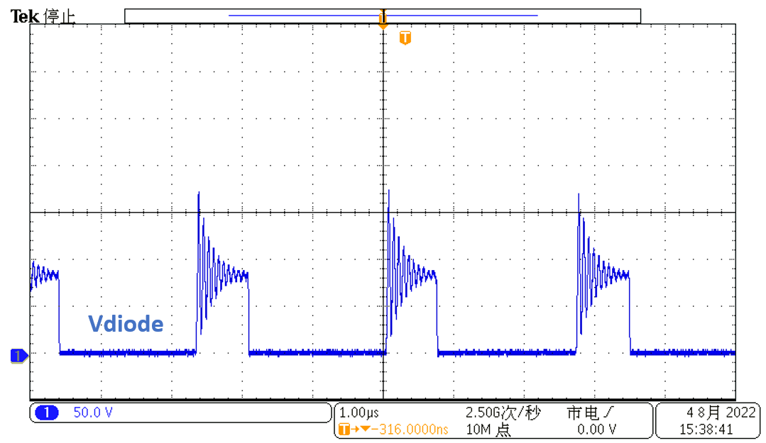
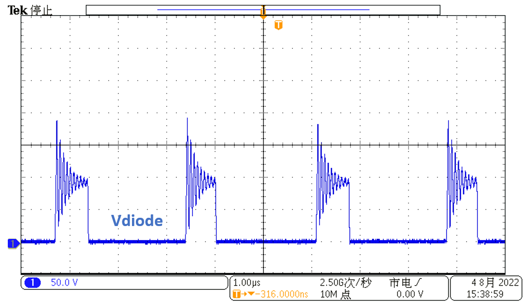
Figure 3-15 through Figure 3-18 show the PMP90994 diode voltage stress waveforms.
 Figure 3-15 Channel A Diode Voltage Stress
VIN = 10 V, IOUT1 = 80 mA, IOUT2 = 80
mA
 Figure 3-16 Channel A Diode Voltage Stress
VIN = 12 V, IOUT1 = 80 mA, IOUT2 = 80
mA
 Figure 3-17 Channel A Diode Voltage Stress
VIN = 18 V, IOUT1 = 80 mA, IOUT2 = 80
mA
 Figure 3-18 Channel A Diode Voltage Stress
VIN = 20 V, IOUT1 = 80 mA, IOUT2 = 80
mA