TIDT296 September   2022


  1.   Description
  2.   Features
  3.   Applications
  4. 1Test Prerequisites
    1. 1.1 Voltage and Current Requirements
    2. 1.2 Required Equipment
  5. 2Testing and Results
    1. 2.1 Efficiency Graphs
    2. 2.2 Cross Regulation
    3. 2.3 Thermal Images
  6. 3Waveforms
    1. 3.1 Start-Up
    2. 3.2 Undervoltage Protection
    3. 3.3 Output Voltage Ripple
    4. 3.4 Load Transients
    5. 3.5 Switching Node Waveforms
    6. 3.6 Short-Circuit Test
    7. 3.7 Diode Voltage Stress

Switching Node Waveforms

The following images show the PMP40994 switching node waveforms.
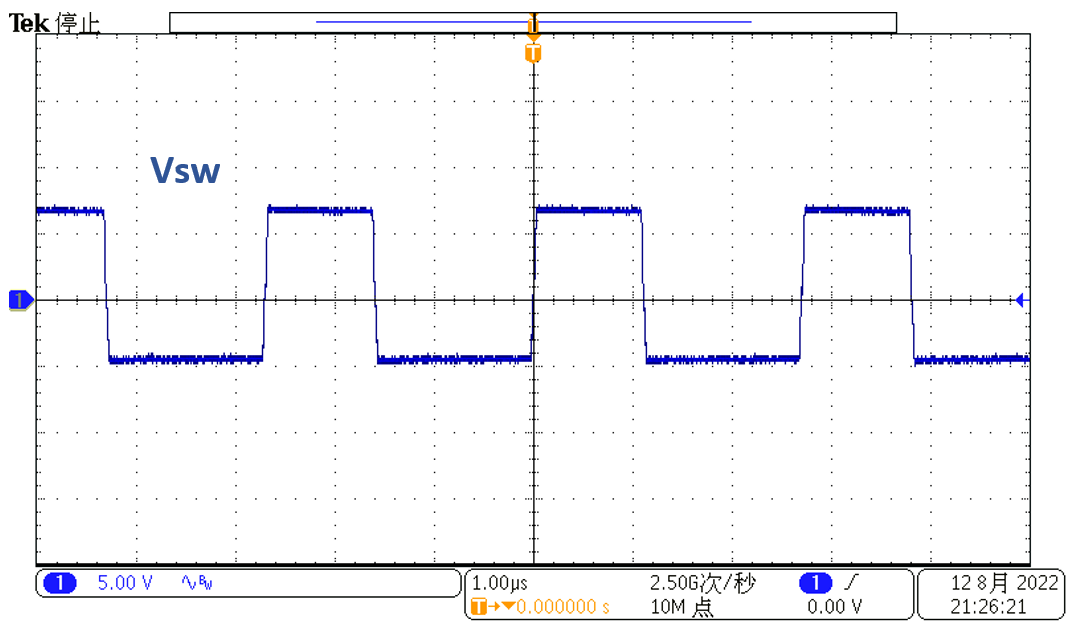
GUID-20220815-SS0I-5F7C-PG00-RXNQQT5P60G1-low.pngFigure 3-11 Switch Node Voltage, VIN = 12 V, IOUT1 = 0 A, IOUT2 = 0 A
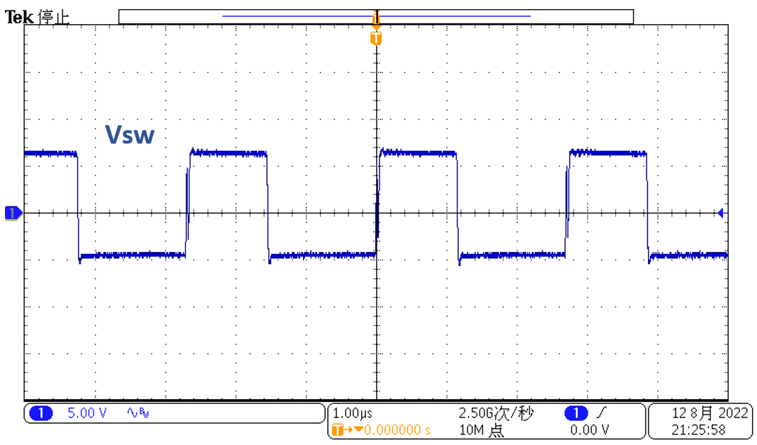
GUID-20220815-SS0I-H7KF-WFW5-5TWBQXBL0DZ5-low.pngFigure 3-12 Switch Node Voltage, VIN = 12 V, IOUT1 = 80 mA, IOUT2 = 80 mA