TIDT320A january 2023 – july 2023
3.5 Bode Plots
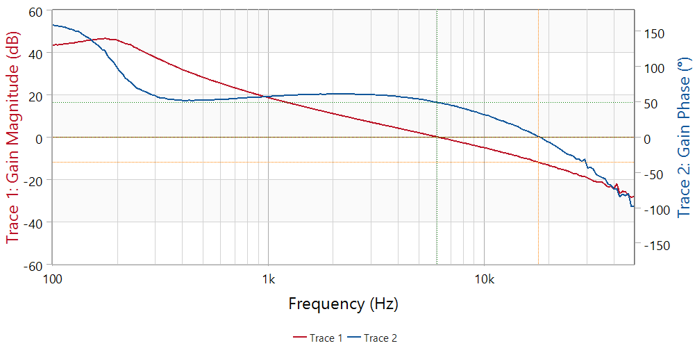
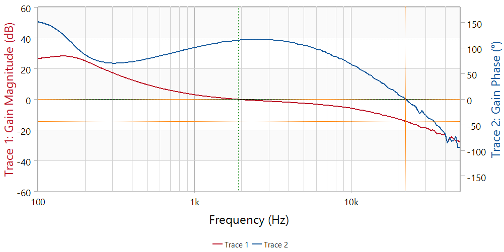
The feedback loop frequency response was measured with 390 VDC input, 3.7-A load on 12VSB and no load on P18V and S12V. Separate measurements were taken with 270 μF of system capacitance and 4700 μF of system capacitance and are shown in the following figures.
Table 3-9 Bode Plot Summary
| System Capacitance (μF) | Phase Margin (°) | Gain Margin (dB) |
|---|---|---|
| 270 | 48.9 | 11.9 |
| 4700 | 116 | 14.3 |
 Figure 3-7 Bode Plot 270-μF System
Capacitance
 Figure 3-8 Bode Plot 4700-μF System
Capacitance