TIDT320A january 2023 – july 2023
2.4 Start-Up Sequence
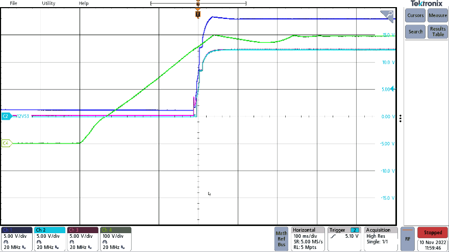
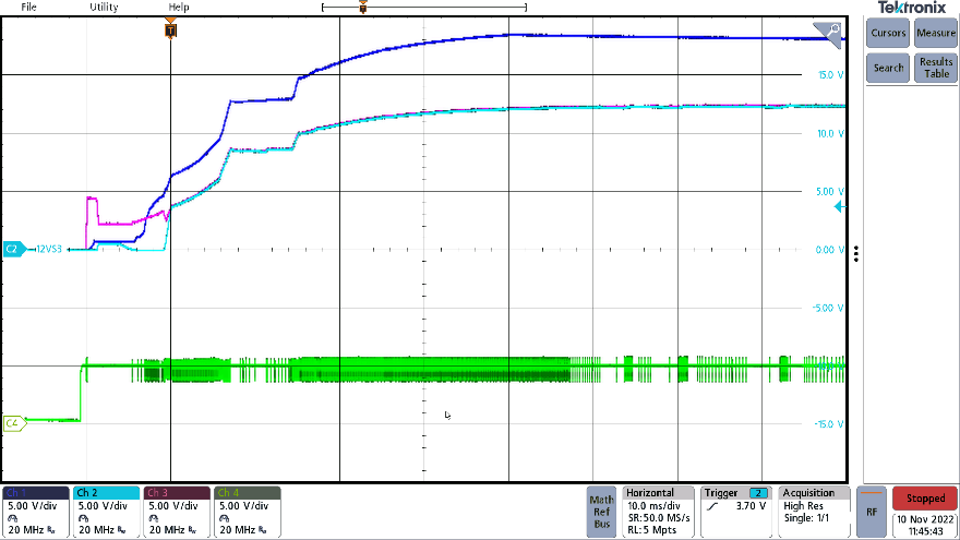
Start-up behavior is shown in the following figures. No load was applied on all outputs, and the input voltage was set to 390 VDC. A system capacitance of 1000-μF was connected to 12VSB, and 100-μF was connected to P18V, respectively. Channel 1 shows the P18V output voltage. Channel 2 shows the 12VSB output voltage. Channel 3 shows the S12V output voltage. Channel 4 shows either the input voltage in Figure 3-27 and the DIS pin voltage in Figure 2-18.
 Figure 2-17 Start-Up (DIS Pin Floating When Input Voltage
is Applied)
 Figure 2-18 Start-Up (Input Voltage Present When DIS Pin
Toggled From 0 V to High-Z)