TIDT320A january 2023 – july 2023
3.1 Efficiency Graphs
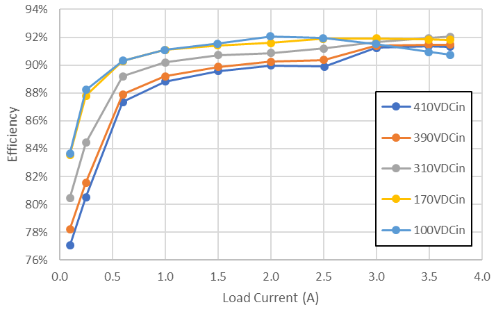
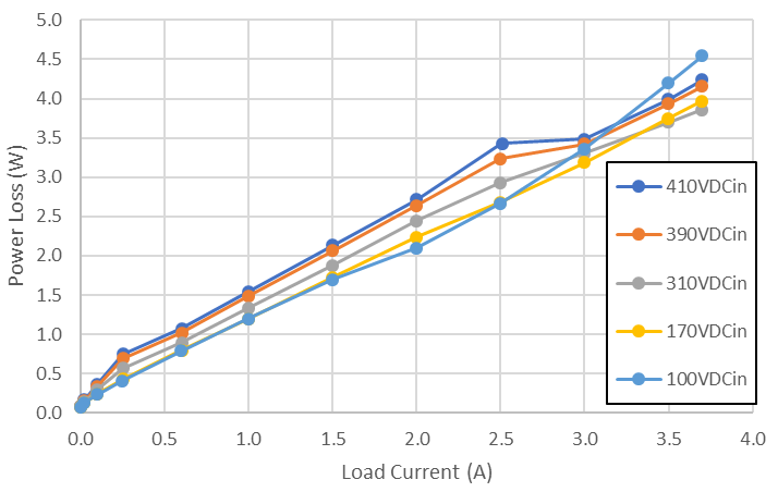
Efficiency was measured with a DC input source and loading only the 12VSB output. Efficiency was recorded with input voltages of 100 VDC, 170 VDC, 310 VDC, 390 VDC, and 410 VDC. Table 3-1 describes the system-level conditions represented by these DC input voltages.
Table 3-1 Rated System-Level Conditions
| DC Input Voltage | Representative System Condition |
|---|---|
| 410 V | PFC pre-regulator maximum output voltage |
| 390 V | PFC pre-regulator nominal output voltage |
| 310 V | Bridge-rectified 230 VAC input voltage |
| 170 V | Bridge-rectified 120 VAC input voltage |
| 100 V | Minimum operating input voltage |
 Figure 3-1 Efficiency Graph
 Figure 3-2 Power Loss Graph