TIDT320A january 2023 – july 2023
2.2 Output Voltage Ripple
The output ripple voltage has a high frequency component due to the switching frequency and a lower frequency component due to the burst frequency in all operating modes except AAM. The following figures show the output ripple in the different modes of operation. A system capacitance of 1000-μF was connected to 12VSB, and 100-μF was connected to P18V, respectively. For all figures, the input was 390 VDC and no load was applied to P18V and S12V.
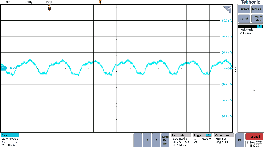 Figure 2-8 Output Voltage Ripple in AAM (3.7 A on
12VSB)
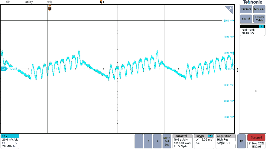 Figure 2-9 Output Voltage Ripple in ABM (2.0 A on
12VSB)
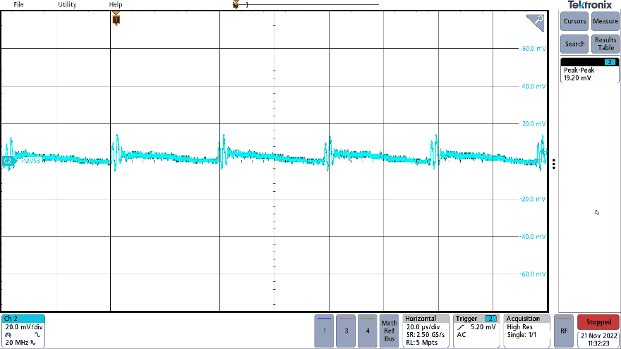 Figure 2-10 Output Voltage Ripple in LPM (250 mA on
12VSB)
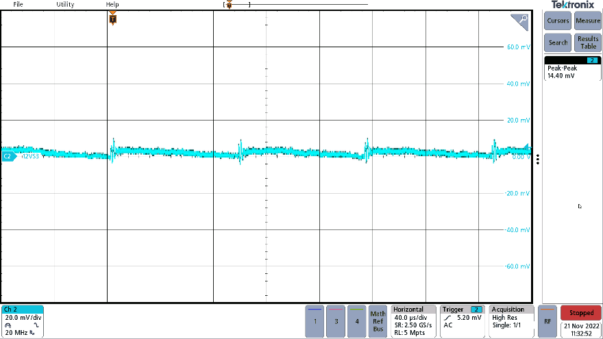 Figure 2-11 Output Voltage Ripple in SBP1 (100 mA on
12VSB)
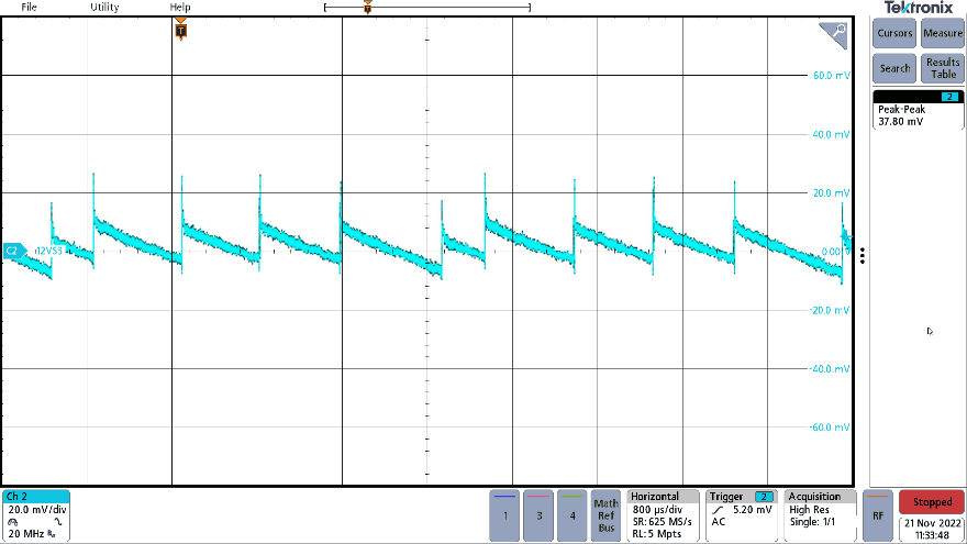 Figure 2-12 Output Voltage Ripple in SBP2 (20 mA on
12VSB)