TIDT320A january 2023 – july 2023
2.3 Load Transients
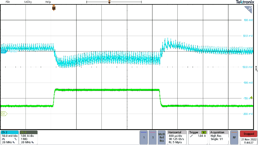
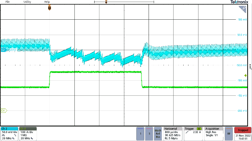
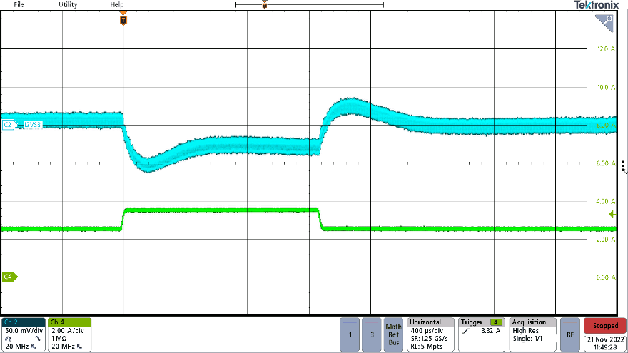
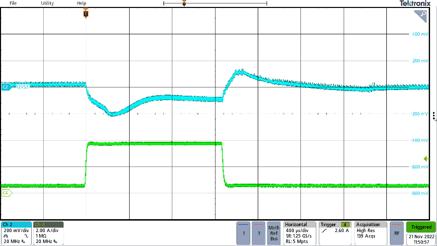
Load transient response is shown in the following figures. The load step was applied to the 12VSB output. The input voltage was 390 VDC, and both P18V and S12V were unloaded. A system capacitance of 1000-μF was connected to 12VSB, and 100-μF was connected to P18V, respectively. Channel 2 shows the 12VSB output voltage, AC coupled. Channel 4 shows the 12VSB load current.
 Figure 2-13 Load Transient (500 mA to 1.5 A)
 Figure 2-14 Load Transient (1.5 A to 2.5 A)
 Figure 2-15 Load Transient (2.5 A to 3.5 A)
 Figure 2-16 Load Transient (500 mA to 3.7 A)