TIDT320A january   2023  – july 2023


  1.   1
  2.   Description
  3.   Features
  4.   Applications
  5. 1Test Prerequisites
    1. 1.1 Voltage and Current Requirements
    2. 1.2 Functional Block Diagram
    3. 1.3 Pin Functions
  6. 2Waveforms
    1. 2.1 Switching Frequency and Operating Modes
    2. 2.2 Output Voltage Ripple
    3. 2.3 Load Transients
    4. 2.4 Start-Up Sequence
  7. 3Testing and Results
    1. 3.1 Efficiency Graphs
    2. 3.2 Efficiency Data
    3. 3.3 No Load and OFF State Power Consumption
    4. 3.4 Thermal Images
    5. 3.5 Bode Plots
    6. 3.6 Load Regulation

Load Regulation

The data from the 390 VDC input efficiency measurements was used to generate the 12VSB and S12V regulation plot shown in Figure 3-27. No additional loading was applied to P18V and S12V.

The second plot (Figure 3-10) shows the voltage measured on P18V for different loading combinations on all outputs.
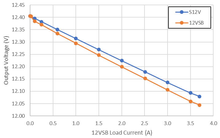
GUID-20230105-SS0I-BLKD-S884-GWVB7BZMQK8K-low.png Figure 3-9 12VSB and S12V Output Voltage Regulation
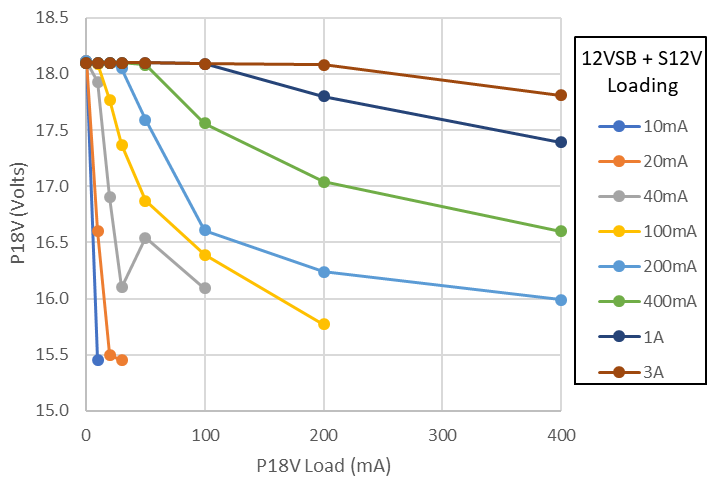
GUID-20230105-SS0I-HFPG-QZ5T-KHLBXLRQPQSP-low.png Figure 3-10 P18V Output Voltage Regulation