TIDT321 January   2023


  1.   Description
  2.   Features
  3.   Applications
  4. 1Test Prerequisites
    1. 1.1 Voltage and Current Requirements
    2. 1.2 Required Equipment
    3. 1.3 Dimensions
  5. 2Testing and Results
    1. 2.1 Efficiency and Load Regulation Graphs
    2. 2.2 Thermal Images
    3. 2.3 Bode Plots
  6. 3Waveforms
    1. 3.1 Switching
    2. 3.2 Output Voltage Ripple
    3. 3.3 Load Transients
    4. 3.4 Start-Up Sequence
    5. 3.5 Other Waveforms

Other Waveforms

Other behavior is shown in the following figures.

Figure 3-9 and Figure 3-10 have input voltage = 630 VDC and output power = full load.
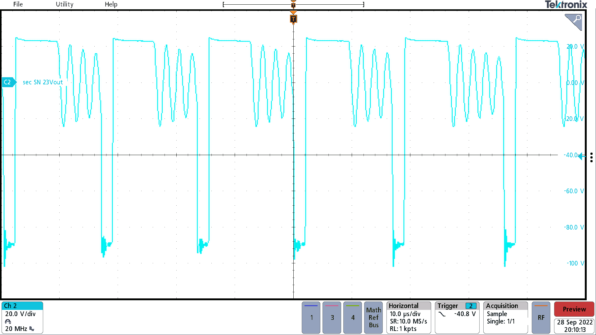
GUID-20221220-SS0I-WMRJ-R8G9-KXNZ6D53WFT9-low.png Figure 3-9 Secondary Side Switch Node 23-V Output
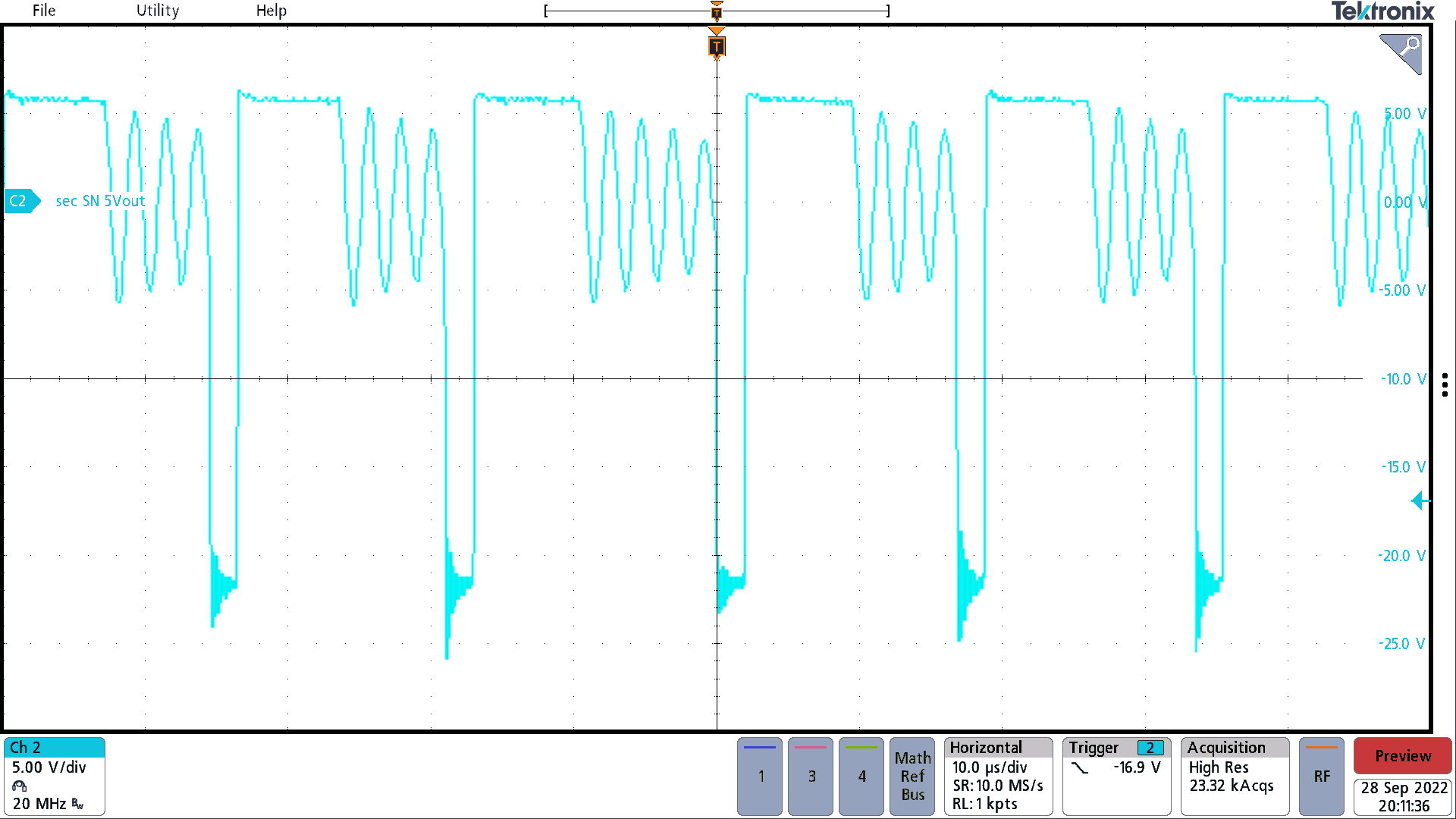
GUID-20221220-SS0I-THVT-177F-T1TWQQNCS90H-low.png Figure 3-10 Secondary Side Switch Node 5-V Output