TIDT333 may 2023
3.1 Switching
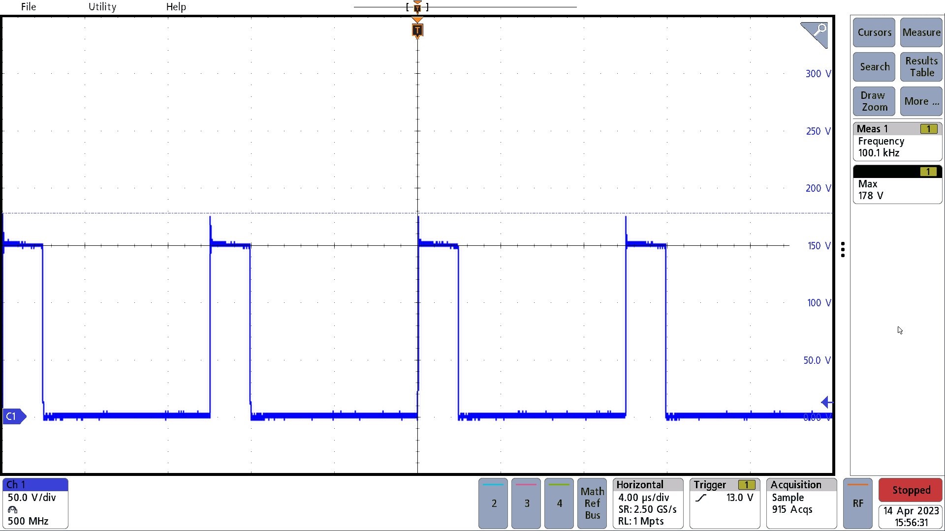
The maximum voltage stress on the drain of the low-side FETs (Q3 and Q4) occurs with 150-V input and 5-A load. This was recorded as 178 Vpk, as shown in the following figure.
 Figure 3-1 Maximum Voltage Stress
TIDT333 may 2023
The maximum voltage stress on the drain of the low-side FETs (Q3 and Q4) occurs with 150-V input and 5-A load. This was recorded as 178 Vpk, as shown in the following figure.
 Figure 3-1 Maximum Voltage Stress