TIDT333 may 2023
2.3 Thermal Images
All images captured with the unit under test (UUT) enclosed in a 30 m × 45 cm × 20 cm Plexiglas box, 25ºC ambient, after a 30-minute warm up, and no forced airflow. The unit was tested with a 5-A load and at various input voltages. Black electrical tap was placed on top of U for increased emissivity.
| Reference Designator | Description | 50 VIN Maximum Temperature (°C) | 100 VIN Maximum Temperature (°C) | 150 VIN Maximum Temperature (°C) |
|---|---|---|---|---|
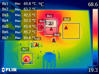
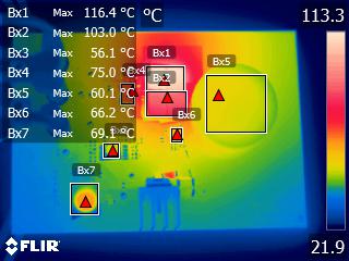
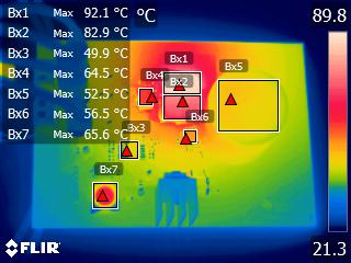
| Q1 and Q2 | High-side FETs | 69.8 | 92.1 | 116.4 |
| Q3 and Q4 | Low-side FETs | 63.7 | 82.9 | 82.9 |
| U2 | TPS7H5001-SP controller | 42.5 | 49.9 | 56.1 |
| U1 | MOSFET driver | 53.5 | 64.5 | 75.0 |
| L1 | Output inductor | 43.4 | 52.5 | 60.1 |
| U3 | INA901-SP current sense amplifier | 45.7 | 56.5 | 66.2 |
| U4 | LM117H linear regulator | 60.6 | 65.6 | 69.1 |
 Figure 2-3 Thermal Image, 50
VIN
 Figure 2-5 Thermal Image, 150
VIN
 Figure 2-4 Thermal Image, 100
VIN