TIDT339 june   2023


  1.   1
  2.   Description
  3.   Features
  4.   Applications
  5. 1Test Prerequisites
    1. 1.1 Voltage and Current Requirements
    2. 1.2 Required Equipment
    3. 1.3 Testing Conditions
    4. 1.4 Considerations
    5. 1.5 Dimensions
  6. 2Testing and Results
    1. 2.1 Efficiency Graphs and Data
      1. 2.1.1 Efficiency Graph: Light Load Performance
      2. 2.1.2 Efficiency Graph: Available Output Power Versus Input Power
      3. 2.1.3 Efficiency Graph: Full Load Performance
      4. 2.1.4 Efficiency Data
        1.       17
        2.       18
        3.       19
    2. 2.2 Thermal Images
    3. 2.3 Static Output Voltage Variation versus Load
      1. 2.3.1 Light Load Range
      2. 2.3.2 Light to Full Load Range
    4. 2.4 EMI Measurement According to EN55022 Class-B Quasi-Peak Limits
  7. 3Waveforms
    1. 3.1 Switching on Q1 (VDS Voltage) at Full Load
    2. 3.2 Output Voltage Ripple
    3. 3.3 Load Transients
    4. 3.4 Start-Up and Shutdown Sequence
      1. 3.4.1 Start-Up Sequence
        1. 3.4.1.1 Load Current 0 A
        2. 3.4.1.2 Load Current 1.7 A
      2. 3.4.2 Shutdown Sequence

Switching on Q1 (VDS Voltage) at Full Load

The switching waveforms were measured by supplying the converter at maximum VIN of 265 VAC with 1.7-A load current.
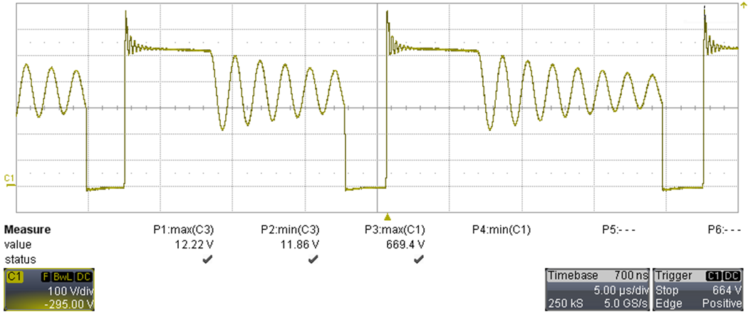
GUID-20230622-SS0I-DCTR-Z3J3-NQ3CZP1LXNHX-low.png Figure 3-1 Waveform Q1-VDS (100 V/div, 5 µs/div, 200 MHz BWL)

The image in Figure 3-2 is the same measurement as in Figure 3-1 but with time base of 1 µs/div to enlarge the overshoot.
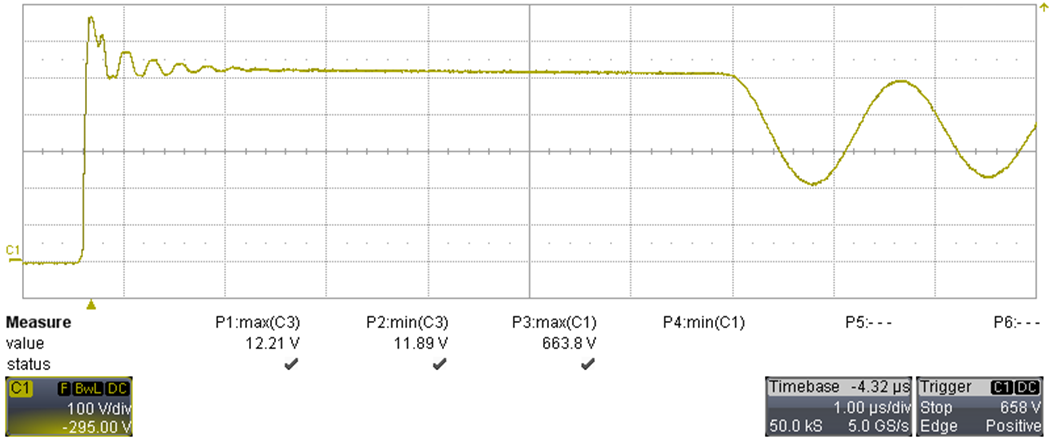
GUID-20230622-SS0I-SHSN-BVN7-0RSSMBSXLFSD-low.png Figure 3-2 Waveform Q1-VDS (100 V/div, 1 µs/div, 200 MHz BWL)