TIDT339 june   2023


  1.   1
  2.   Description
  3.   Features
  4.   Applications
  5. 1Test Prerequisites
    1. 1.1 Voltage and Current Requirements
    2. 1.2 Required Equipment
    3. 1.3 Testing Conditions
    4. 1.4 Considerations
    5. 1.5 Dimensions
  6. 2Testing and Results
    1. 2.1 Efficiency Graphs and Data
      1. 2.1.1 Efficiency Graph: Light Load Performance
      2. 2.1.2 Efficiency Graph: Available Output Power Versus Input Power
      3. 2.1.3 Efficiency Graph: Full Load Performance
      4. 2.1.4 Efficiency Data
        1.       17
        2.       18
        3.       19
    2. 2.2 Thermal Images
    3. 2.3 Static Output Voltage Variation versus Load
      1. 2.3.1 Light Load Range
      2. 2.3.2 Light to Full Load Range
    4. 2.4 EMI Measurement According to EN55022 Class-B Quasi-Peak Limits
  7. 3Waveforms
    1. 3.1 Switching on Q1 (VDS Voltage) at Full Load
    2. 3.2 Output Voltage Ripple
    3. 3.3 Load Transients
    4. 3.4 Start-Up and Shutdown Sequence
      1. 3.4.1 Start-Up Sequence
        1. 3.4.1.1 Load Current 0 A
        2. 3.4.1.2 Load Current 1.7 A
      2. 3.4.2 Shutdown Sequence

Output Voltage Ripple

The output voltage ripple was measured by supplying the converter at 230 VAC, while loaded at 1.7 A; the bandwidth limit of oscilloscope (BWL) was set to 20 MHz.
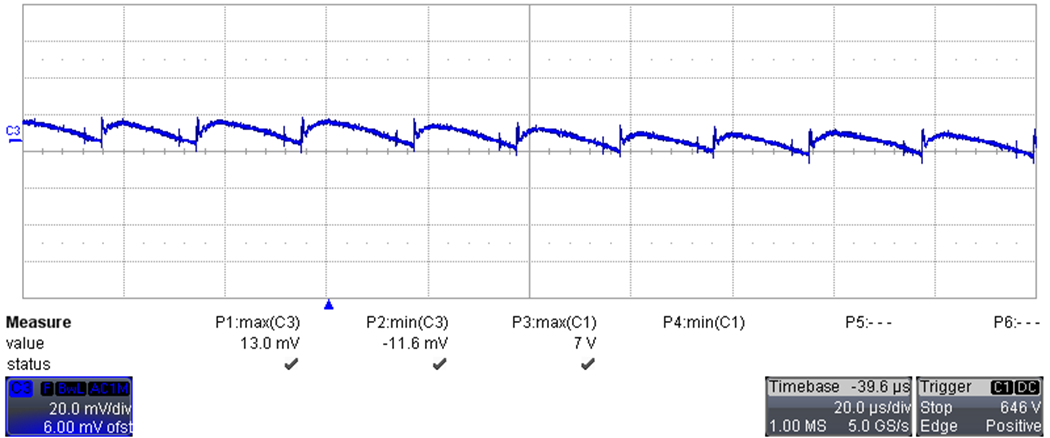
GUID-20230622-SS0I-ND4C-QJ73-SMSGDH550HSL-low.png Figure 3-3 Output Voltage (20 mV/div, 20 µs/div, AC coupling)


Figure 3-4 is the same measurement as in Figure 3-3 but with longer time division, showing details about low frequency ripple.
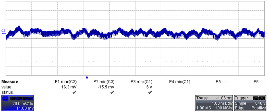
GUID-20230622-SS0I-97XP-83Q4-DH03ZLTG8V5T-low.png Figure 3-4 Output Voltage (20 mV/div, 1 ms/div, AC coupling)