TIDT361 December   2023


  1.   1
  2.   Description
  3.   Features
  4.   Applications
  5. 1Test Prerequisites
    1. 1.1 Voltage and Current Requirements
    2. 1.2 Dimensions
  6. 2Testing and Results
    1. 2.1 Efficiency Graphs
    2. 2.2 Efficiency Data
    3. 2.3 Thermal Images
  7. 3Waveforms
    1. 3.1 Switching
    2. 3.2 Output Voltage Ripple
    3. 3.3 Load Transients
    4. 3.4 Start-up Sequence

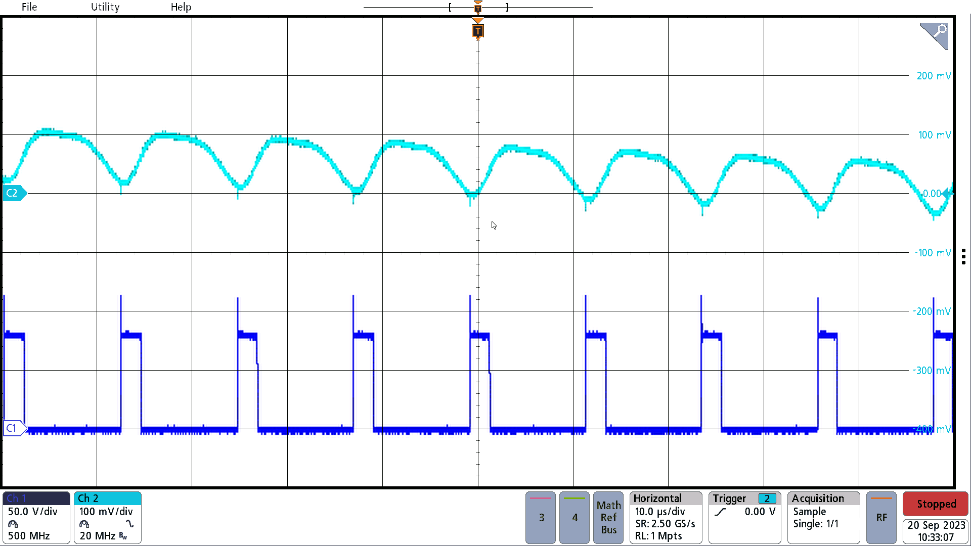
Output Voltage Ripple

Output voltage waveforms along with switching node are shown in the following images.

  • Channel 1 (blue): Switching node
  • Channel 2 (cyan): Output (AC coupled)
GUID-20231208-SS0I-SVV2-VJ33-BMKXFVSNVKZN-low.png Figure 3-2 40-Vdc Input
GUID-20231208-SS0I-DCGX-S1VM-0WCCNFHGPN7Z-low.png Figure 3-3 80-Vdc Input