TIDT369B November   2023  – July 2024


  1.   1
  2.   Description
  3.   Features
  4.   Applications
  5.   Resources
  6. 1System Description
    1. 1.1 System Block Diagram
    2. 1.2 Key System Specification
    3. 1.3 Design Consideration
      1. 1.3.1 Boost Inductor Design
      2. 1.3.2 High Frequency Power Switch Selection
      3. 1.3.3 Input AC Voltage Sensing
      4. 1.3.4 Bulk Voltage Sensing
      5. 1.3.5 Input Current Sensing
      6. 1.3.6 Baby Boost Design
      7. 1.3.7 Relay
      8. 1.3.8 Protection
        1. 1.3.8.1 Over Voltage Protection
        2. 1.3.8.2 Over Current Protection
  7. 2Download Firmware
  8. 3Power Up
    1. 3.1 Required Equipment
    2. 3.2 Considerations
    3. 3.3 Start-Up Sequence
  9. 4Testing Results
    1. 4.1 Start-Up Waveform
    2. 4.2 THD Performance
    3. 4.3 Power Factor
    4. 4.4 Efficiency
      1. 4.4.1 Efficiency Graph
      2. 4.4.2 Efficiency Data
    5. 4.5 E-meter Performance
      1. 4.5.1 E-meter Graphs
      2. 4.5.2 E-meter Data
    6. 4.6 Load Transients
    7. 4.7 Input Current Waveforms
    8. 4.8 AC Drop Test
    9. 4.9 Thermal Images
  10. 5External Reference

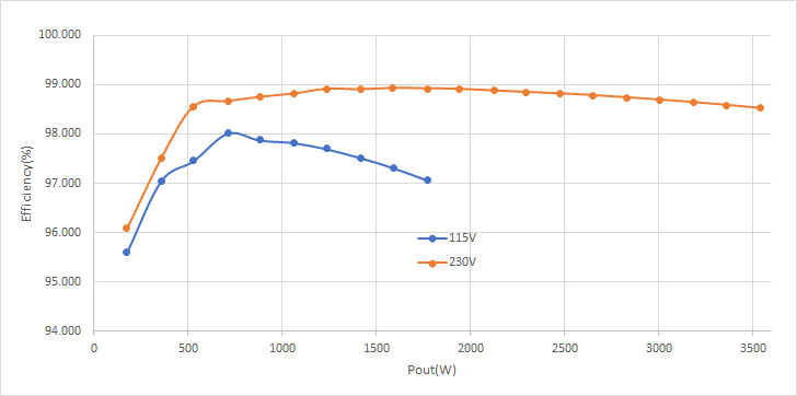
Efficiency Graph

Conditions

  • Switching Frequency: 65kHz
  • GaN Slew Rate: 100V/ns
  • Output: 385V
  • Power analyzer: WT5000
  • Relay and BB bypass FETs shorted
  • Auxiliary supply not included
PMP23338 Efficiency GraphFigure 4-7 Efficiency Graph