TIDT375 December 2023
3.1 Switching
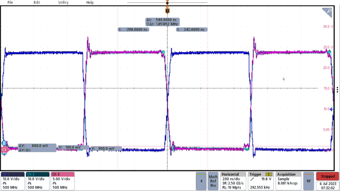
Switching behavior is shown in the following figure. Channel 1 and 2 are the primary side switching nodes. Channel 3 is the synchronous rectifier switching node. Test conditions for the waveform shown are 48-V input and no load.
 Figure 3-1 Switching Nodes