TIDT383 March 2024
3.1 Switching
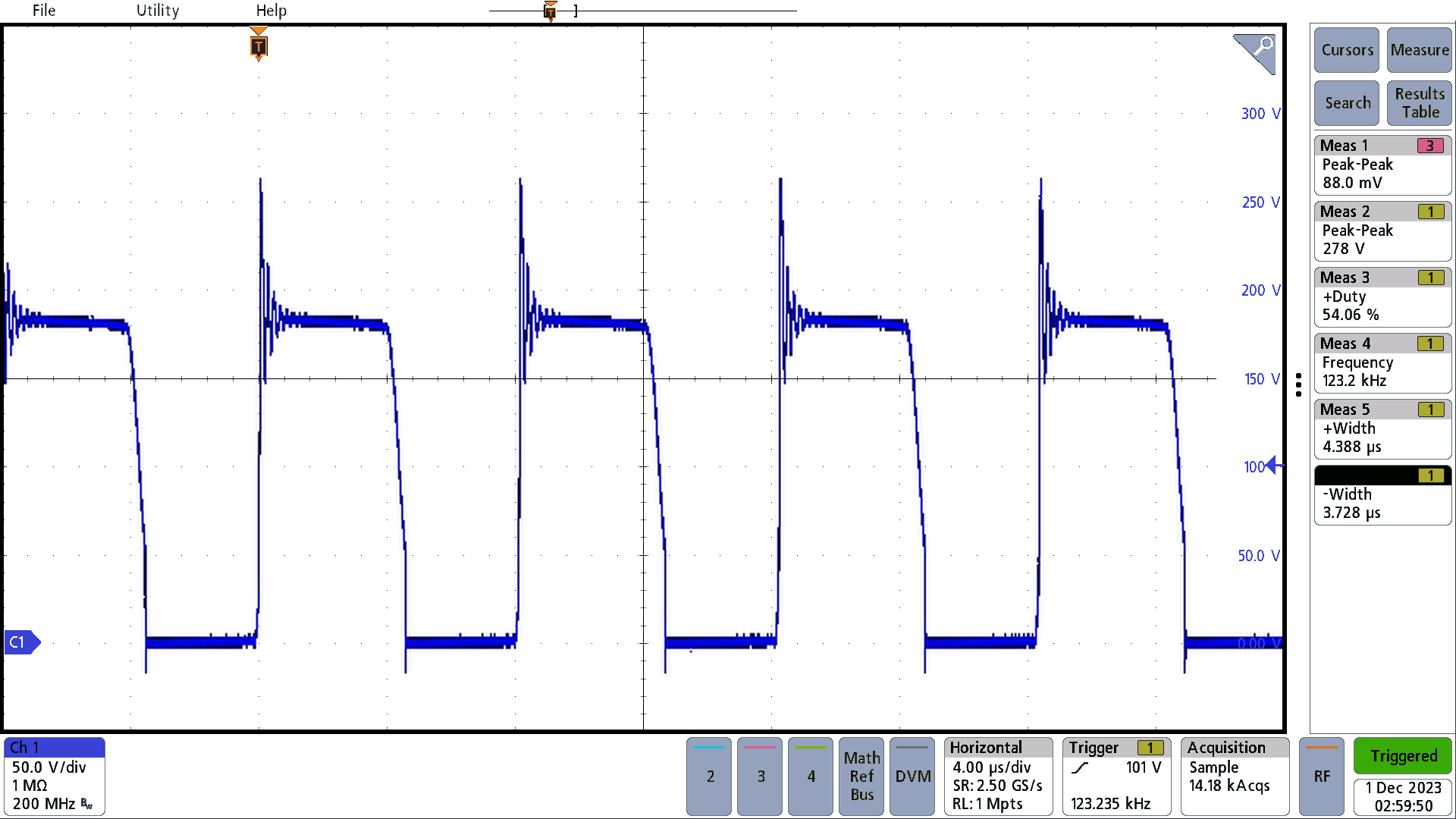
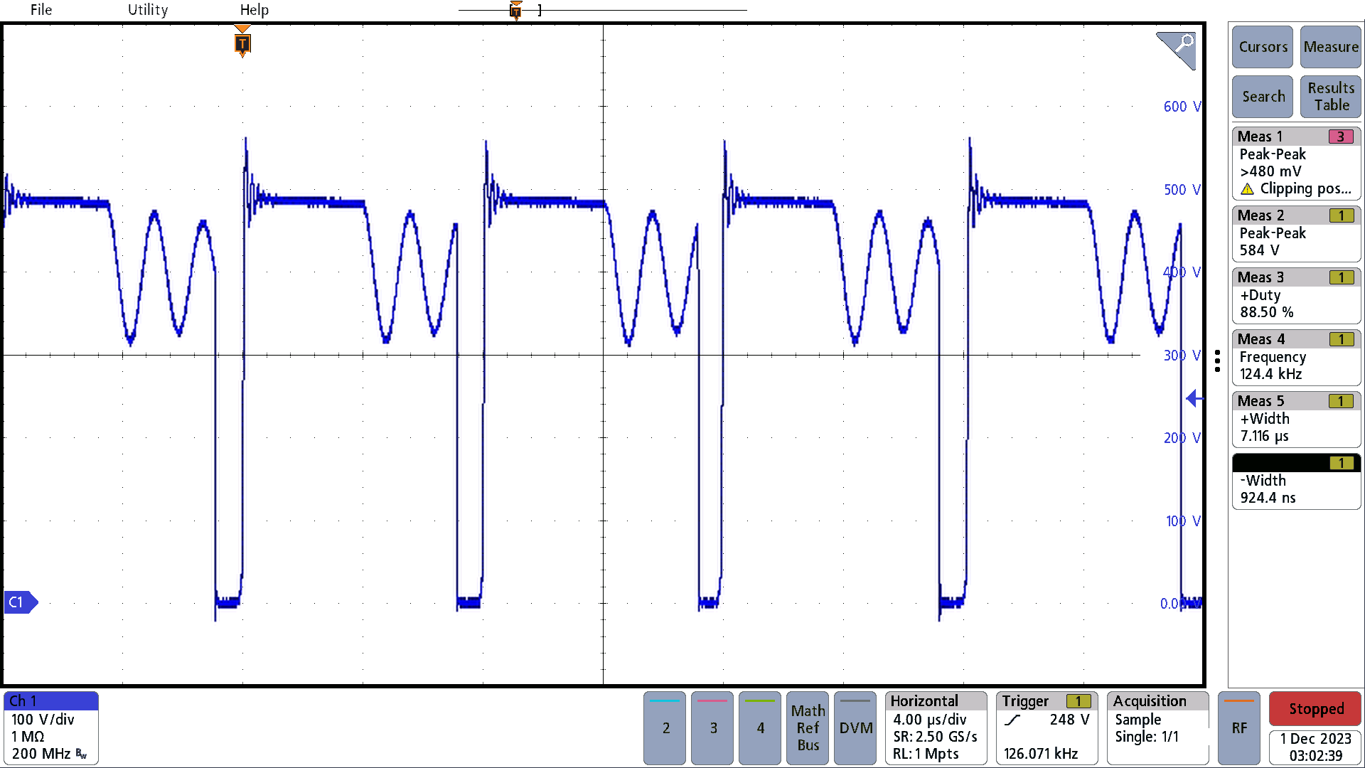
The images below show key switching waveforms. The waveforms are measured with 12V, 0.25A; 12V, 0.0094A; and 12V, 0.25A full load.
 Figure 3-1 Primary Switch
Node - Full Load, 100VDC In
 Figure 3-2 Primary Switch
Node - Full Load, 400VDC In