TIDT383 March 2024
3.2 Output Voltage Ripple
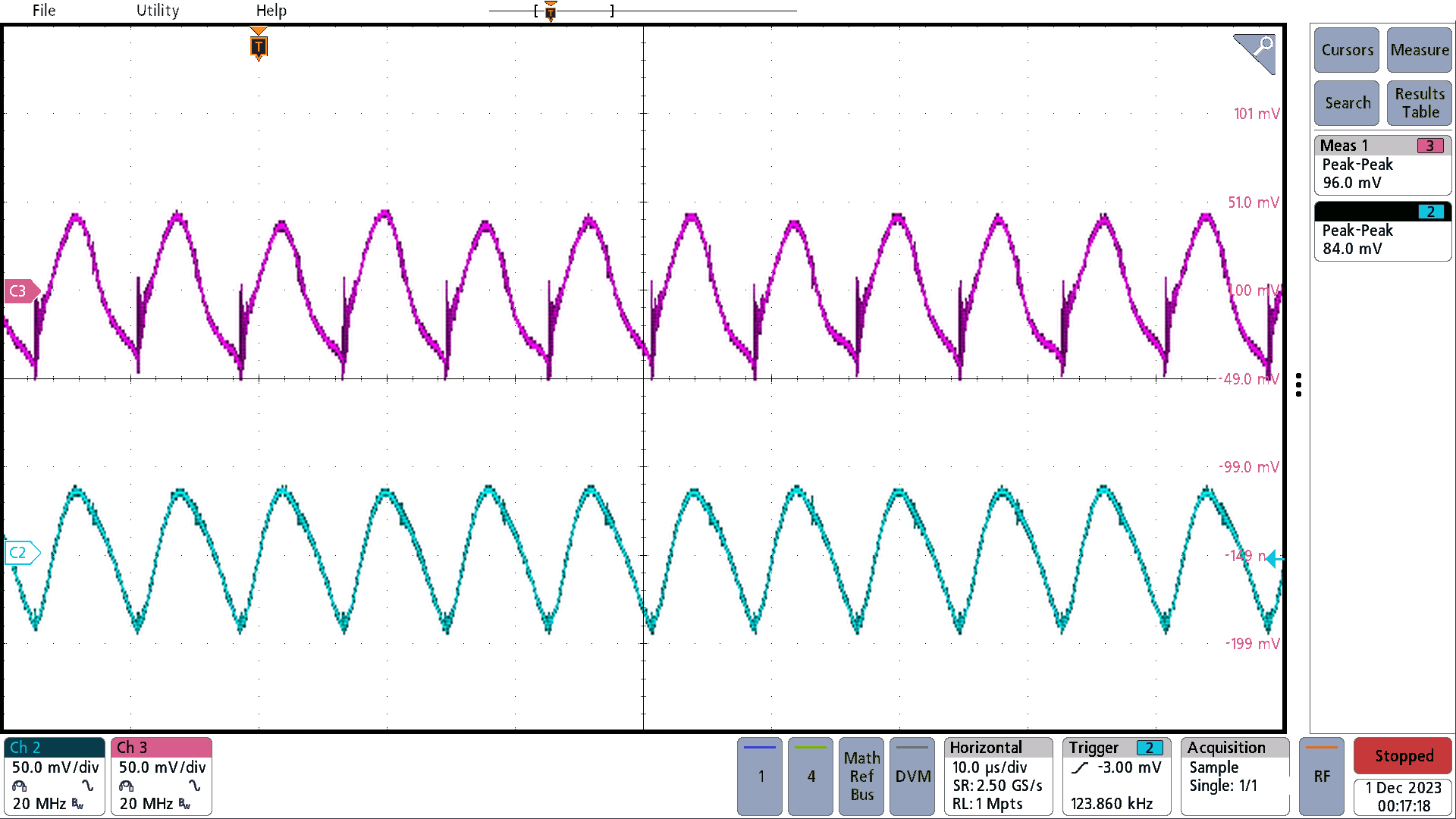
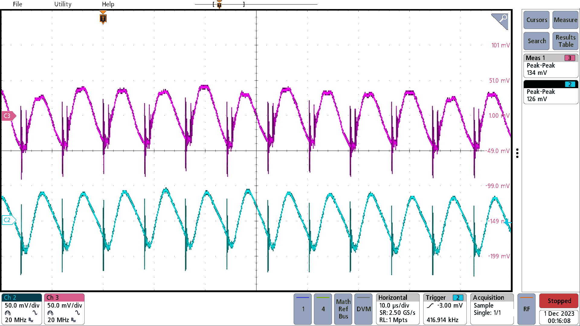
The output ripple voltages are shown in the plots below at 12V, 0.25A; 12V, 0.094A; 12V, 0.25A full load.

Ch3: Vp (Regulated Output)
Ch2: Vs (Unregulated Output)
Figure 3-3 Output Ripple - Full Load,
100VDC InCh2: Vs (Unregulated Output)

Ch3: Vp (Regulated Output)
Ch2: Vs (Unregulated Output)
Figure 3-4 Output Ripple - Full Load,
400VDC InCh2: Vs (Unregulated Output)