TIDT412A October 2024 – November 2024
3.6 Overvoltage Protection
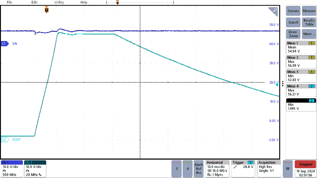
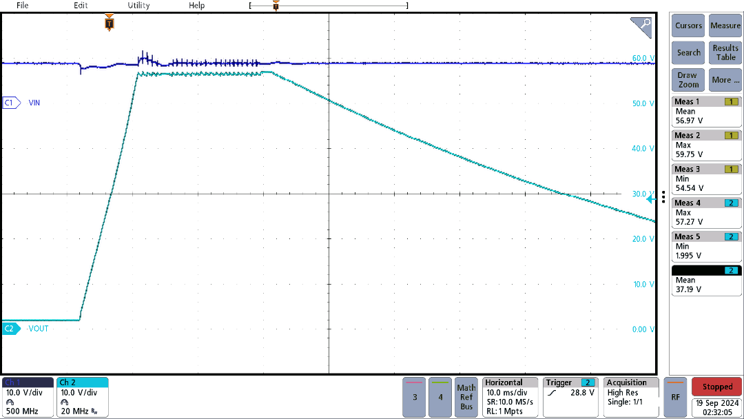
Figure 3-13 and Figure 3-14 show one of the protection features of the front-end of this design, overvoltage protection. The LM74930-Q1 is set to an overvoltage clamp configuration, where LM74930-Q1 retries passing through the input voltage until the capacitor on the TMR pin is charged up, then falls to 0V.
Figure 3-13 shows operation at 55V of input voltage, while Figure 3-14 shows operation at 57V of input voltage. At the higher input voltage, the hysteresis frequency is more apparent.
 Figure 3-13 Overvoltage Protection at
55VIN
 Figure 3-14 Overvoltage Protection at
57VIN
Figure 3-14 Overvoltage Protection at
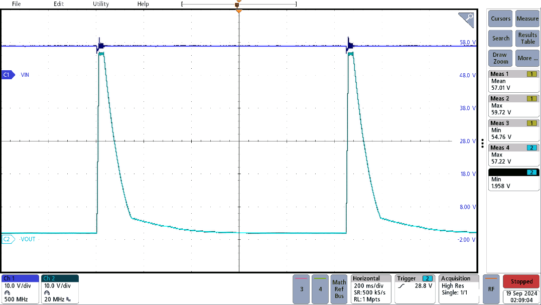
57VINFigure 3-15 shows the frequency at which the system retries start-up after the input voltage has been completely blocked. This measurement shows operation at 57V, but is similar across input voltage.
 Figure 3-15 Overvoltage Protection at
57VIN – Zoomed Out